Preparation method and failure analysis method for transmission electron microscope (TEM) sample

A technology of samples and failure points, which is applied in the field of TEM sample preparation, can solve the problems that cannot be achieved, and abnormal areas cannot be found.

Active Publication Date: 2014-07-09
WUHAN XINXIN SEMICON MFG CO LTD
View PDF5 Cites 37 Cited by
  • Summary
  • Abstract
  • Description
  • Claims
  • Application Information

AI Technical Summary

Problems solved by technology

[0006] However, due to the limitation of the resolution of the FIB machine, when the thickness of a specific layer in a semiconductor device such as an ultra-thin gate oxide layer is too small (for example, less than 3nm), it cannot be observed by the FIB machine, and naturally the specific layer cannot be found abnormal region
In this way, the purpose of extracting TEM samples that contain abnormal areas and can be observed and analyzed by TEM machines in the roughly located failure positions cannot be achieved

Method used


Image

  • Preparation method and failure analysis method for transmission electron microscope (TEM) sample
  • Preparation method and failure analysis method for transmission electron microscope (TEM) sample
  • Preparation method and failure analysis method for transmission electron microscope (TEM) sample

Examples


preparation example Construction

[0029] The preparation method and failure analysis method of the TEM sample provided by the present invention include the following steps:

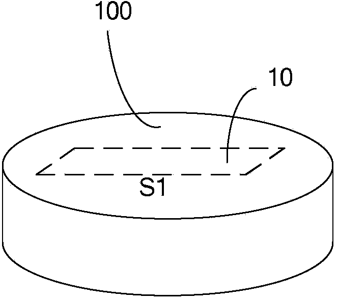
[0030] S1: Perform rough positioning on the substrate 100, find the failure area 10 and mark the range of the failure area 10 on the substrate 100.

[0031] Such as figure 1 As shown, the substrate 100 is a semiconductor substrate, which may be monocrystalline silicon, polycrystalline silicon, or amorphous silicon, or silicon, germanium, silicon germanium compound, gallium arsenide, etc., and the semiconductor substrate 100 may also have an epitaxial layer Or the silicon structure on the insulating layer, or other semiconductor materials, which are not listed here. In the substrate 100, there are a plurality of completed semiconductor devices to be inspected.

[0032] The rough positioning of the substrate 100 is intended to find the problematic semiconductor device and the approximate failure area in the device, that is, the failure area 10. ...


PUM

PropertyMeasurementUnit
lengthaaaaaaaaaa

Abstract

The invention provides a preparation method and failure analysis method for a transmission electron microscope (TEM) sample. The method comprises the following steps: performing rough positioning on a failure area on a substrate, cutting an initial sample comprising the failure area, accurately positioning a specific failure point in the initial sample by using the TEM, and thinning the initial sample to form a final sample, namely the TEM sample for TEM electronic penetration can be provided. Therefore, the technical problems that a focused ion beam (FIB) is insufficient in resolution ratio, a failure point on a specific layer with small enough thickness inside a semiconductor cannot be accurately positioned and a TEM sample cannot be manufactured in the traditional technology are solved.

Description

Technical field [0001] The invention relates to the field of semiconductors, in particular to a method for preparing a TEM sample and a failure analysis method. Background technique [0002] In the semiconductor production process, it is inevitable that there will be problems in the process of forming some semiconductor devices on the substrate, such as uneven film deposition thickness during the deposition process. Therefore, it is necessary to inspect the internal structure of the semiconductor device in real time during the production process to remove the defective device or part of the device and find the cause of the problem to facilitate subsequent production. [0003] At present, the commonly used method is to extract a sample for transmission electron microscopy (TEM) observation from the substrate, and use TEM to observe the cross section of the TEM sample to find the location of the failure point, and the phenomenon caused by the failure location, and carry out the failu...

Claims


Application Information

Patent Timeline
Patent Type & Authority Applications(China)
IPC IPC(8): G01N1/28G01N23/04
Inventor 郭伟仝金雨李剑李桂花
Owner WUHAN XINXIN SEMICON MFG CO LTD
Why Eureka
Try Eureka