Method for manufacturing high-performance double-layer polysilicon bipolar transistor

A technology of bipolar transistor and manufacturing method, applied in transistor, semiconductor/solid-state device manufacturing, semiconductor device and other directions, can solve the problem of increasing base-emitter distance, reducing current amplification factor, reducing emitter current conduction area, etc. The problem is to reduce the high temperature process time, increase the current amplification factor, and reduce the buried layer doping and the expansion effect.

Active Publication Date: 2014-07-09
NO 55 INST CHINA ELECTRONIC SCI & TECHNOLOGYGROUP CO LTD
View PDF5 Cites 9 Cited by
  • Summary
  • Abstract
  • Description
  • Claims
  • Application Information

AI Technical Summary

Problems solved by technology

The advantage of the dielectric side wall structure is that the isolation effect is good, and the disadvantage is that the current conduction area of ​​the emitter is reduced, that is, the emitter resistance is increased.
The reason is that for a high-performance double-layer polysilicon BJT, the P+ polysilicon spacing is generally 0.6 μm to 1.0 μm (not too large, too large will increase the b...

Method used


Image

  • Method for manufacturing high-performance double-layer polysilicon bipolar transistor
  • Method for manufacturing high-performance double-layer polysilicon bipolar transistor
  • Method for manufacturing high-performance double-layer polysilicon bipolar transistor

Examples


Embodiment

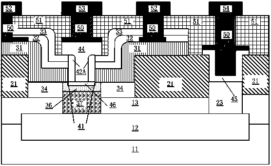
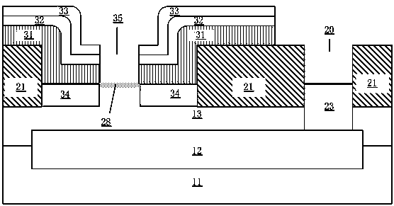
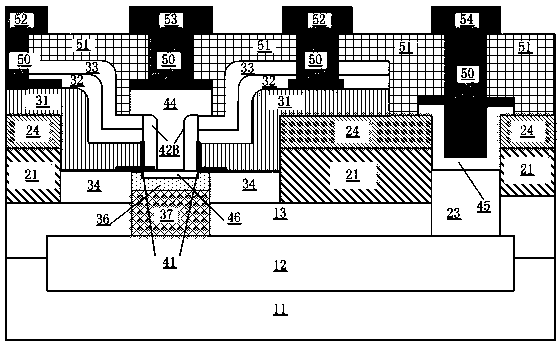
[0067] 1) Select the silicon substrate material 11, its doping is P-type, and the resistivity is 30Ω. cm; Sb atoms are selectively implanted on the substrate to form an N+ buried layer 12, followed by N-type silicon epitaxy 13, with a resistivity of 8Ω. cm, and the thickness of the epitaxial layer is 1.5 μm. ( Figure 2.2 )

[0068] 2) Oxidation to form thin SiO 2 layer 14, thickness 300?, after which deposited Si 3 N4 15, thickness 1000?, photolithography and dry etching of Si 3 N 4 , forming a local oxidation window, high temperature oxidation after degumming, to obtain LOCOS 21, thickness 5000?, oxidation temperature 1050 ℃, time 45 minutes, peel off Si after oxidation 3 N 4 . ( Figure 2.3 , Figure 2.4 )

[0069] 3) Lithograph the collector region 22, and implant phosphorus (P) atoms into the collector region with a dose of 5×10 15 / cm 2 , the energy is 150KeV, forming a low-resistance channel 23 . ( Figure 2.5 )

[0070] 4) CVD deposited SiO 2 , with a...


PUM


Abstract

The invention discloses a method for manufacturing a high-performance double-layer polysilicon bipolar transistor. The method comprises the following steps that 1), LOCOS and CVD are adopted to deposit SiO2 to form a composite isolation structure, and high-temperature process time is reduced; 2), the SiO2 is used as an etching stopping layer of base polysilicon, and etching damage is avoided; 3), a composite side wall structure is formed through SiO2 and N+polysilicon, and emitter resistance is reduced. The method has the advantages that on the premise of not lowering the isolation effect, the high-temperature process time is reduced, therefore, a relatively thin epitaxial layer can be adopted, the better microwave performance is obtained, SiO2 is adopted as the etching stopping layer, the etching damage to the silicon epitaxial layer is eliminated, breakdown characteristics are improved, current amplifying coefficients are increased, and noise coefficients are reduced. The composite side wall structure with SiO2 and N+polysilicon is adopted, it can be guaranteed that emitter-base electric isolation is carried out, and meanwhile the emitter resistance is lowered, the current amplifying coefficients are increased, and the noise coefficients are reduced.

Description

technical field [0001] The invention relates to a method for manufacturing a high-performance double-layer polysilicon bipolar transistor, which belongs to the technical field of microelectronic design and manufacture. Background technique [0002] At present, in the field of wired and wireless communication, compound semiconductor devices, such as GaAs HBT or HEMT, SiGe HBT, etc., have high cut-off frequency and low noise figure due to their inherent material characteristics, and are used in low-noise amplifiers and mixers. It has been widely used in circuits such as. Silicon-based devices, due to lower mobility, their high-frequency performance is inferior to the above-mentioned devices, but at the low end of the microwave, in small and medium power amplifiers and mixer applications in RF front-end and baseband circuits, compared with compound low-noise devices , The advantages of silicon-based BJT are low phase noise, mature technology, and low cost, so it has strong mar...

Claims


Application Information

Patent Timeline
IPC IPC(8): H01L21/331H01L29/73
CPCH01L29/6625H01L29/735
Inventor 应贤炜庸安明吕勇王佃利
Owner NO 55 INST CHINA ELECTRONIC SCI & TECHNOLOGYGROUP CO LTD
Why Eureka
Try Eureka