Fin type semiconductor structure and forming method thereof

A semiconductor and fin-type technology, applied in the field of fin-type semiconductor structure and its formation, can solve problems such as high capacitance and large leakage current, and achieve the effects of improving sensitivity, prolonging service life, and improving device performance

Active Publication Date: 2014-07-09
唐棕
View PDF4 Cites 14 Cited by
  • Summary
  • Abstract
  • Description
  • Claims
  • Application Information

AI Technical Summary

Problems solved by technology

[0004] However, due to the characteristics of the substrate structure of the conventional FinFET, there is a problem that the leakage current between the source region and the drain region will be conducted through the substrate. Due to the short gate length, sometimes a large leakage current will be generated.
In addition, there is also a problem of high capacitance between the source drain and the substrate

Method used


Image

  • Fin type semiconductor structure and forming method thereof
  • Fin type semiconductor structure and forming method thereof
  • Fin type semiconductor structure and forming method thereof

Examples


Embodiment 1

[0054] The present invention proposes a semiconductor structure and a manufacturing method thereof, such as Figure 1-16 Shown is a schematic diagram of the intermediate steps of the method. Hereinafter, each step of the embodiment of the present invention will be described in detail with reference to these figures.

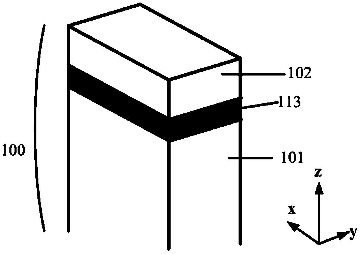
[0055] Step A: Provide a substrate 100 including a sacrificial region, and form a fin substrate 100 having a lower substrate 180 and a fin portion 110 on the substrate, the sacrificial region 113 is in the fin portion, refer to Image 6 shown.

[0056] In the process of preparing the substrate, such as figure 1 As shown, a substrate 100 is provided, the substrate 100 includes a first substrate 101, the material of which can be silicon, and then a sacrificial region 113 is formed on the first substrate 101 by an epitaxy method. In an embodiment, the sacrificial region 113 is a sacrificial layer 113 that runs through the entire substrate. The material of the s...

Embodiment 2

[0085] Only the aspects of the second embodiment that differs from the first embodiment will be described below. Parts not described should be considered to be performed using the same steps, methods or processes as those in the first embodiment, so details will not be repeated here.

[0086] Step A: providing a substrate 100 including a sacrificial region 113 , forming a fin substrate 100 having a lower substrate 180 and a fin portion 110 on the substrate 100 , the sacrificial region 113 being in the fin portion.

[0087] Different from the first embodiment, in this embodiment, the sacrificial region 113 is not a sacrificial layer penetrating the fin portion, but is represented as one or more sacrificial blocks 113 .

[0088] The method of forming the sacrificial block 113 can be completed in the process of preparing the substrate 100. In this embodiment, a substrate 100 is provided, and a mask is formed at the position where the surface of the substrate 100 needs to be prote...

Embodiment 3

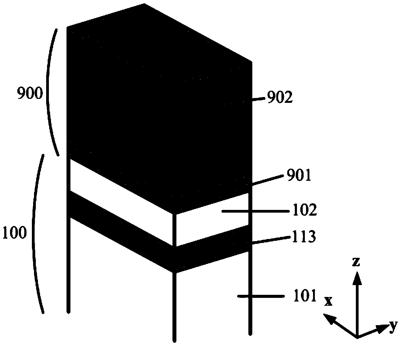
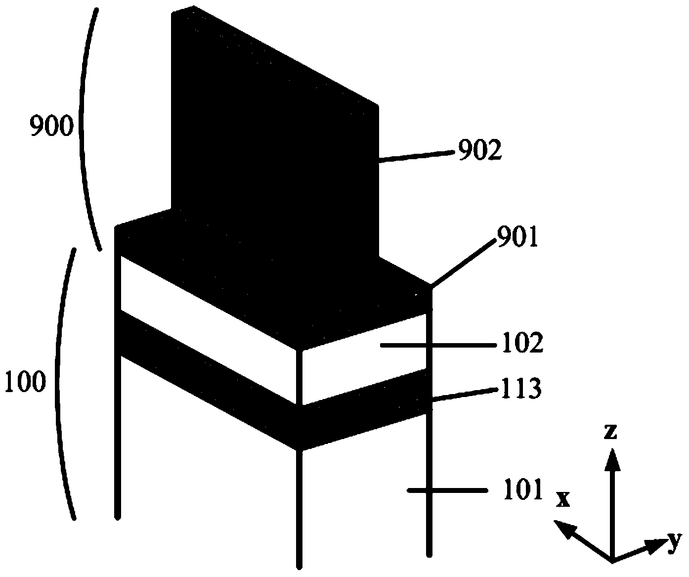
[0095] In addition, the present invention also proposes a fin-type semiconductor device structure, referring to Figure 12, the device has: a fin-shaped substrate 100 including a lower substrate 180 and a fin portion 110, a source region 6002 and a drain region 6001 on the fin portion 110, and the source region 6002 and the drain region 6001 straddle the fin The gate structure 400 on the sheet portion 110, the fin portion below the gate structure is a channel, the shallow trench isolation 105 located on both sides of the fin portion 110 in the y direction and below the gate structure 400, and the gate structure 405 in the x direction The sidewalls 500 on both sides of the structure 400, and the isolation region 300 formed in the fin portion 110 between the channel and the lower substrate. The fin part 110 may include an upper fin part 114 , a sacrificial region 113 and a lower fin part 112 . The width of the top surface of the fin portion 110 is preferably 1-10 nm, and the cr...


PUM


Abstract

The invention provides a fin type semiconductor structure which is capable of effectively controlling leakage currents between a source region and a drain region and improving gate control capacity. The fin type semiconductor structure comprises a fin type substrate, the source region, the drain region, a gate structure, shallow ridge isolation parts and an isolation region, wherein the fin type substrate is provided with a lower substrate and a fin part, the source region and the drain region are formed on the fin part, the gate structure is formed between the source region and the drain region and stretches across the fin part, the shallow ridge isolation parts are formed on the two sides of the fin part and are located below the gate structure, and the isolation region is formed in the fin part. The isolation region can be basically located below the source region and / or basically located below the drain region, and / or basically located below the gate structure. The invention further provides a method for forming the fin type semiconductor structure.

Description

technical field [0001] The present invention relates to the technical field of semiconductor design and manufacture thereof, in particular to a fin-type semiconductor structure and a forming method thereof. Background technique [0002] FinFET is called Fin Field-Effect Transistor (Fin Field-Effect TransistorFinFET), which is a new complementary metal oxide semiconductor (CMOS) transistor. Fin means fish fin. FinFET is named according to the similarity between the shape of the transistor and the fish fin. Other similar names include Tri-gate MOS and so on. [0003] FinFET is an innovative design derived from the current traditional standard field-effect transistor (Field-Effect TransistorFET). In the traditional transistor structure, the gate that controls the flow of current can only control the on and off of the circuit on one side of the gate, which belongs to the planar structure. In the FinFET structure, the gate is formed into a fork-shaped 3D structure similar to a ...

Claims


Application Information

Patent Timeline
Patent Type & Authority Applications(China)
IPC IPC(8): H01L29/78H01L29/10H01L21/336
CPCH01L29/1083H01L29/66795H01L29/785H01L29/7854
Inventor 李迪
Owner 唐棕
Why Eureka
Try Eureka