A Compact Ultra-Wideband Dual-Trap Balanced Bandpass Filter

A filter and ultra-wideband technology, applied in waveguide-type devices, electrical components, circuits, etc., can solve the problems of cumbersome common-mode response design, poor common-mode rejection characteristics, complex internal circuit structure, etc., to achieve low cost, convenient Processed, compact effect

Inactive Publication Date: 2015-12-02
NANJING UNIV OF AERONAUTICS & ASTRONAUTICS
View PDF3 Cites 1 Cited by
  • Summary
  • Abstract
  • Description
  • Claims
  • Application Information

AI Technical Summary

Problems solved by technology

[0004] At present, there are mainly three methods for the design of balanced bandpass filters: the first is a balanced filter based on a double-sided parallel stripline structure, which has good common-mode rejection characteristics, but the internal circuit structure is complex and the size is large. The production cost is very high; the second is a balanced filter based on the microstrip ladder impedance coupled line structure, the design of its differential mode response is relatively simple, and it has good common mode rejection characteristics, but the design of its common mode response is cumbersome, And it has great limitations for broadband applications; the third is a balanced filter based on the balance of the bandpass filter of the microstrip short-circuit branch line, which has good differential-mode in-band characteristics and in-band common-mode rejection characteristics. And the design idea is relatively simple, but its disadvantage is that the out-of-band rejection performance in the differential mode and the common-mode rejection performance in the ultra-wideband state are not good

Method used


Image

  • A Compact Ultra-Wideband Dual-Trap Balanced Bandpass Filter
  • A Compact Ultra-Wideband Dual-Trap Balanced Bandpass Filter
  • A Compact Ultra-Wideband Dual-Trap Balanced Bandpass Filter

Examples


Embodiment Construction

[0031] specific implementation plan

[0032] Below in conjunction with accompanying drawing, the implementation of technical scheme is described in further detail:

[0033] Both the output port and the input port of the balanced filter of the present invention are welded with SMA heads, so as to be connected to test or to be connected with other circuits.

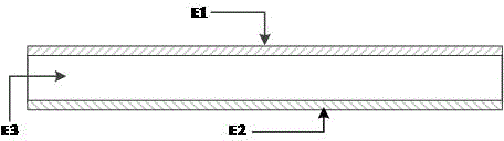
[0034] The present invention uses the RT / Duriod5880 board with a relative dielectric constant of 2.2, a thickness of 0.508mm, and a loss factor of 0.0009 as the substrate, and a PCB of other specifications may also be used as the substrate. Such as figure 1As shown, the upper and lower surfaces of the dielectric substrate E3 of the PCB are covered with an upper metal layer E1 and a lower metal layer E2 respectively. The upper microstrip line structure of the balanced filter of the present invention is the upper metal layer E1, and the slot line structure is formed by etching on the lower layer metal E2.
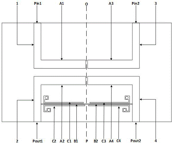
[0035] figure...


PUM


Abstract

The invention discloses a compact type UWB dual-band trap balancing band-pass filter, and belongs to the technical field of wireless communications. The compact type UWB dual-band trap balancing band-pass filter comprises a first filter, a second filter and supplement structures. The first filter and the second filter are in structural symmetry and respectively comprise a microstrip line structure formed on the upper layer of a dielectric substrate and a trough line structure formed on the lower layer of the dielectric substrate. In order to restrain common-mode harmonic waves and achieve dual-band trap characteristics, the supplement structures are additionally arranged in the microstrip line structures on the upper layers of the dielectric substrates, each supplement structure comprises a first microstrip branch knot, a second microstrip branch knot, a first harmonic oscillator, a second harmonic oscillator, a third harmonic oscillator and a fourth harmonic oscillator, wherein the first harmonic oscillator and the second harmonic oscillator are arranged on the two sides of the first microstrip branch knot in parallel, and the third harmonic oscillator and the fourth harmonic oscillator are arranged on the two sides of the second microstrip branch knot in parallel. The compact type UWB dual-band trap balancing band-pass filter has a wide different-mode signal passband and has the dual-band trap characteristics, a high common-mode restraining characteristic is achieved in the passband, the structure is compact, circuits are simple, and processing is easy.

Description

technical field [0001] The invention relates to the technical field of wireless communication, in particular to a compact ultra-wideband dual-band notch balanced bandpass filter. Background technique [0002] The rapid development of modern communication systems puts forward higher requirements on the performance of filters. Miniaturized, high-performance, and wide-band filters are an indispensable part of communication systems. The balanced filter can effectively suppress the internal noise and environmental noise of the system, and has greater advantages compared with the ordinary single-ended filter. [0003] When the relative bandwidth exceeds 100%, the design of a broadband or ultra-wideband balanced bandpass filter not only needs to ensure low insertion loss, but also realizes the transmission of ultra-wideband differential-mode signals, and needs to suppress ultra-wideband common-mode signals, and Keep the filter compact. Therefore, how to increase the differential-...

Claims


Application Information

Patent Timeline
Patent Type & Authority Patents(China)
IPC IPC(8): H01P1/20H01P1/203
Inventor 邓宏伟赵永久苏培贺莹
Owner NANJING UNIV OF AERONAUTICS & ASTRONAUTICS
Why Eureka
Try Eureka