Organic light emitting diode panel and device and preparation, short-circuit detection and short-circuit reparation method of organic light emitting diode panel

A technology of organic light-emitting panel and organic light-emitting layer, which is applied in the direction of measuring device, circuit, measuring electricity, etc., can solve the problem of production line being polluted and so on.

Active Publication Date: 2014-07-16
SHANGHAI TIANMA MICRO ELECTRONICS CO LTD +1
View PDF7 Cites 13 Cited by
  • Summary
  • Abstract
  • Description
  • Claims
  • Application Information

AI Technical Summary

Problems solved by technology

[0004] In order to solve the phenomenon that in the Array manufacturing process, the mixed use of negative photoresist glue to prepare isolation columns may easily cause the production line to be polluted, the present invention provides an organic light-emitting panel and device with a simple preparation method and low cost, a preparation method and its Detection method

Method used


Image

  • Organic light emitting diode panel and device and preparation, short-circuit detection and short-circuit reparation method of organic light emitting diode panel
  • Organic light emitting diode panel and device and preparation, short-circuit detection and short-circuit reparation method of organic light emitting diode panel
  • Organic light emitting diode panel and device and preparation, short-circuit detection and short-circuit reparation method of organic light emitting diode panel

Examples


Embodiment 1

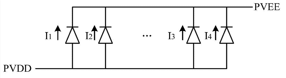
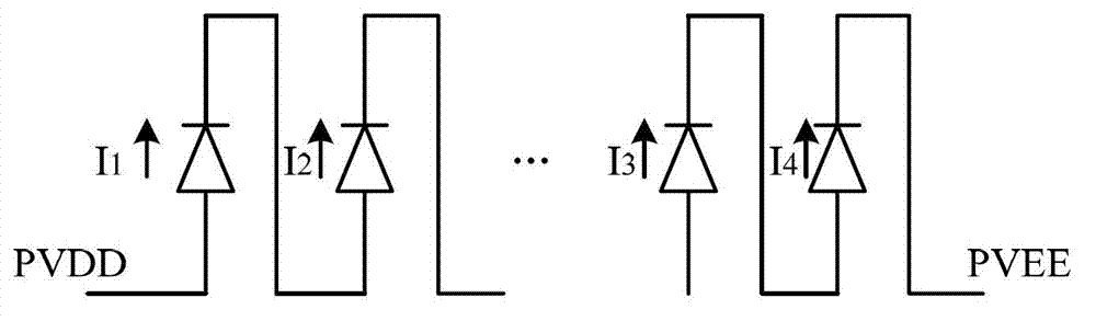
[0071] Such as Figure 2a-2dAs shown, the present invention discloses an organic light-emitting OLED panel, comprising: a substrate 10 ; and a plurality of adjacent light-emitting units located on the substrate 10 . In the figure, only two adjacent light emitting units are shown, that is, the first light emitting unit 11 and the second light emitting unit 22 , other light emitting units are not shown. The organic light-emitting OLED panel further includes a third electrode 31 located between adjacent light-emitting units (ie, the first light-emitting unit 11 and the second light-emitting unit 22 ). Of course, since only two adjacent light emitting units are shown in the figure, a third electrode may also be provided between the second light emitting unit and the adjacent light emitting unit (not shown in the figure). It also includes a connection wire M for connecting the first light emitting unit 11 and the second light emitting unit 22 .

[0072] refer to Figure 2d The f...

Embodiment 2

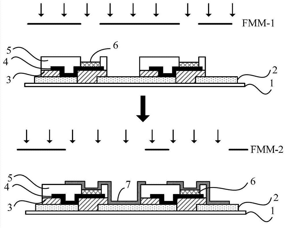
[0079] On the basis of the above-mentioned embodiments, Embodiment 2 of the present invention discloses a method for preparing an organic light-emitting OLED panel. The preparation process is as follows: Figure 2a-2d shown. Its specific preparation process is:

[0080] providing a substrate 10;

[0081] Such as Figure 2a , 2a’ As shown, a first conductive layer (not shown in the figure) is sequentially formed on the substrate 10, and the first conductive layer is patterned to form at least two adjacent first electrodes 120, 220 (in this embodiment, only two adjacent second electrodes as an example, but not limited thereto), the third electrode 31 located between the adjacent first electrodes 120, 220, and the third electrode 31 connected to one of the adjacent first electrodes 120, 220 The connection line M of the first electrode, the third electrode includes a first edge A1 extending from the bottom edge N of the third electrode 31;

[0082] Such as Figure 2b As show...

Embodiment 3

[0087] On the basis of the above embodiments, the present invention discloses another embodiment, such as Figures 3a-3e As shown, the present invention discloses an organic light-emitting OLED panel, including: a substrate 110 ; and a plurality of adjacent light-emitting units located on the substrate 110 . In the figure, only two adjacent light-emitting units, ie, the first light-emitting unit 101 and the second light-emitting unit 201 , are shown, and other light-emitting units are not shown. The organic light-emitting OLED panel further includes a third electrode 112 located between adjacent light-emitting units (ie, the first light-emitting unit 101 and the second light-emitting unit 201 ). Of course, since only two adjacent light emitting units are shown in the figure, a third electrode 212 may also be provided between the second light emitting unit and the adjacent light emitting unit (not shown in the figure).

[0088] Wherein the first light-emitting unit 101 include...


PUM


Abstract

The invention discloses an organic light emitting diode panel and device which is simple in preparation method and low in cost, and a preparation, short-circuit detection and short-circuit reparation method of the organic light emitting diode panel. The OLED panel comprises two or more light emitting units and one or more third electrodes, wherein each third electrode comprises an edge comprising a first edge extending out of the bottom side of the third electrode, and second electrodes of the adjacent light emitting units are positioned on the same layer and are disconnected at the edges of the third electrodes. Due to the fact that the light emitting units in the organic light emitting diode panel are connected in series, uniformity of integral brightness is ensured. The preparation method is simple and feasible. An ordinary open mask is adopted during preparation of the second electrodes, yield during technological process is ensured, cost is low, good operability is achieved, production cost is reduced, and production efficiency is increased.

Description

technical field [0001] The invention relates to the field of OLED (Organic Light-Emitting Diode) lighting, in particular to an organic light-emitting panel and an organic light-emitting device, as well as a method for preparing the organic light-emitting panel, a short-circuit detection method, and a short-circuit repair method. Background technique [0002] Generally, the light emitting principle of an organic light-emitting diode (OLED) light-emitting device is that electrons are injected into the light-emitting layer (EML) from an electron injection electrode (cathode), and holes are injected into the EML from a hole injection electrode (anode). The holes and electrons injected into the EML recombine in the EML to generate energy and excite electrons. Therefore, when electrons transition from an excited state to a ground state, light is generated along with it, enabling the OLED light emitting device to emit light. At present, there are two schemes for panel design of OL...

Claims


Application Information

Patent Timeline
Patent Type & Authority Applications(China)
IPC IPC(8): H01L27/32H01L51/52H01L51/56G01R31/02
Inventor 顾寒昱曾章和钱栋张通
Owner SHANGHAI TIANMA MICRO ELECTRONICS CO LTD
Why Eureka
Try Eureka