
LED epitaxial layer, growth method thereof and LED chip

A technology of LED chip and growth method, which is applied in the direction of electrical components, circuits, semiconductor devices, etc., can solve the problems of low luminous efficiency of LED chips, achieve the effects of inhibiting lateral growth, improving luminous efficiency, and increasing the number of quantum dots

Inactive Publication Date: 2014-07-16
XIANGNENG HUALEI OPTOELECTRONICS
View PDF3 Cites 11 Cited by
  • Summary
  • Abstract
  • Description
  • Claims
  • Application Information

AI Technical Summary

Problems solved by technology

[0004] The purpose of the present invention is to provide an LED epitaxial layer and its growth method and LED chips, so as to solve the technical problem of low luminous efficiency of LED chips in the prior art

Method used


Image

  • LED epitaxial layer, growth method thereof and LED chip
  • LED epitaxial layer, growth method thereof and LED chip
  • LED epitaxial layer, growth method thereof and LED chip

Examples


example 2

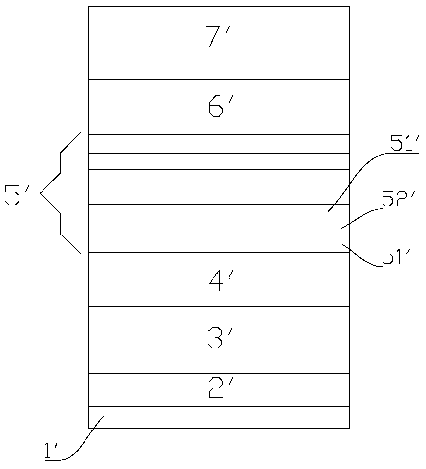
[0032] The LED epitaxial layer of example 2 is as image 3 shown. The difference between Example 2 and Example 1 is that a unit structure of the MQW layer 5 is a Mg-doped layer 53 disposed on the top surface of the N-type confinement layer 4 . The InGaN layer 51 is disposed on the top surface of the Mg-doped layer 53 . GaN layer 52 is provided on the top surface of InGaN layer 51 .

example 3

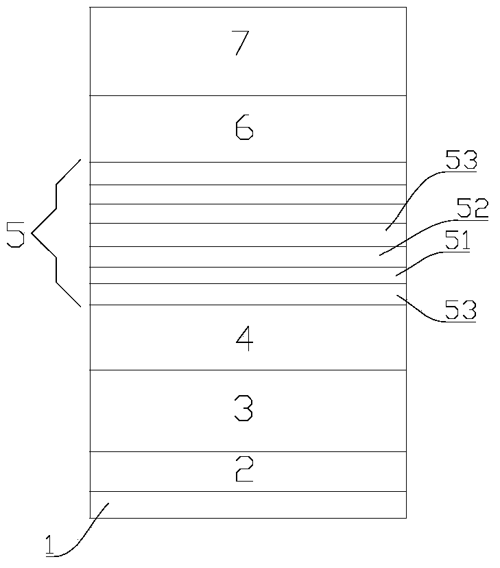
[0033] The LED epitaxial layer of example 3 is as Figure 4shown. The difference between Example 3 and Example 1 is that a unit structure of the MQW layer 5 is an InGaN layer 51 disposed on the top surface of the N-type confinement layer 4 . A magnesium-doped layer 53 is provided on the top surface of the InGaN layer 51 . GaN layer 52 is disposed on top of magnesium-doped layer 53 .

[0034] Most preferably, the magnesium-doped layer 53 in the structural unit is grown on the top surface of the N-type confinement layer 4 , the InGaN layer 51 is grown on the top surface of the magnesium-doped layer 53 , and the GaN layer 52 is grown on the top surface of the InGaN layer 51 . At this time, the luminous efficiency of the LED epitaxial layer increases the most.

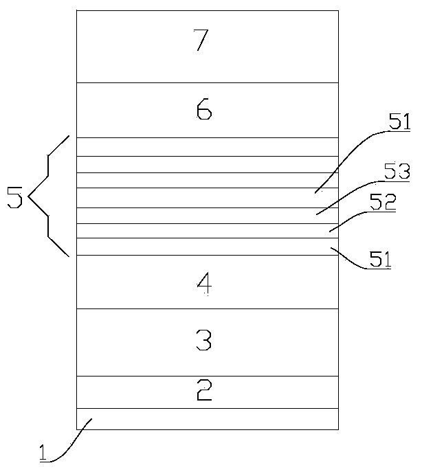
[0035] The structures mentioned in Examples 1-3 can increase the number of quantum dots in the InGaN layer 51 when growing it, thereby improving the luminous efficiency of the LED epitaxial layer. Each layer outside th...

Embodiment 1

[0063] 1. Process the sapphire substrate for 17 minutes at 1100°C and maintain the reaction chamber pressure at 200mbar in a hydrogen atmosphere;

[0064] 2. Cool down to 550°C, keep the pressure in the reaction chamber at 300mbar, and feed NH at the same time 3 , TMGa grows a buffer GaN layer 2 with a thickness of 30 nm on the sapphire substrate 1;

[0065] 3. Raise the temperature to 1100°C, maintain the pressure in the reaction chamber at 200mbar, and feed NH at the same time 3 , TMGa, growing a 2 μm undoped GaN layer 3;

[0066] 4. Then feed NH at the same time 3 , TMGa, SiH 4 N-type GaN doped with Si is grown, the Si doping concentration is 1E+19, and the total thickness is controlled at 2-4 μm to obtain an N-type confinement layer 4;

[0067] 5. The pressure of the reaction chamber is maintained at 300mbar, and Cp2Mg and NH are introduced at the same time 3 MgN crystal nuclei with a thickness of 1.0 nm are grown for 50 seconds to obtain a magnesium-doped layer 53 ; ...


PUM


Abstract

The invention provides an LED epitaxial layer, a growth method of the LED epitaxial layer and an LED chip. The LED epitaxial layer comprises an N-type confinement layer, an MQW layer and a P-type confinement layer, wherein the N-type confinement layer, the MQW layer and the P-type confinement layer grow in order, the MQW layer comprises a plurality of structure units, and each structure unit comprises an InGaN layer and a GaN layer. The LED epitaxial layer is characterized in that the inside of each structure unit further comprises at least one magnesium doping layer. According to the LED epitaxial layer, the magnesium doping layers are additionally arranged in multiple quantum wells, surfaces of GaN potential barriers are coarse, growth of InGaN potential wells is influenced, InGaN cross growth is inhibited, InGaN three-dimensional growth is promoted, and accordingly the number of quantum dots in InGaN is increased, and light-emitting efficiency of the LED chip is improved by 5%-6%.

Description

technical field [0001] The invention relates to the field of LED (Light Emitting Diode), in particular to an LED epitaxial layer, a growth method thereof and an LED chip. Background technique [0002] Quantum dots are quasi-zero-dimensional nanomaterials, composed of a small number of atoms. The three dimensions of quantum dots are all below 100nm. They look like extremely small dots, and the movement of electrons in them is restricted in all directions. Therefore, the confinement effect of quantum dots is particularly significant. Quantum dots have properties intermediate between those of bulk semiconductors and those of discrete molecules. Quantum dots can be used in various applications, for example, in transistors, solar cells, LEDs, diode lasers, as medical imaging agents, as qubits, and as memory. [0003] GaN-based LED blue-green light-emitting devices mostly use InGaN / GaN superlattice multiple quantum well layer (MQW layer) as the light-emitting layer. like figur...

Claims


Application Information

Patent Timeline
Patent Type & Authority Applications(China)
IPC IPC(8): H01L33/06H01L33/00
CPCH01L33/06H01L33/0066H01L33/0075H01L33/325
Inventor 林传强
Owner XIANGNENG HUALEI OPTOELECTRONICS
Learn More