Monocrystalline silicon wafer texturing additive, texturing solution and corresponding texturing method

A technology of monocrystalline silicon wafers and additives, applied in chemical instruments and methods, crystal growth, after treatment, etc., can solve problems such as enlarged pyramid size, low solar cell efficiency, and weakened corrosion rate, and achieve improved stability and consistency Sexuality, cost reduction, and the effect of reducing usage

Inactive Publication Date: 2014-07-23
선테크파워컴퍼니리미티드 +1
View PDF0 Cites 19 Cited by
  • Summary
  • Abstract
  • Description
  • Claims
  • Application Information

AI Technical Summary

Problems solved by technology

Additives such as sodium silicate are currently used in the texturing process, and their ability to improve the interfacial tension between the silicon wafer and the solution is relatively poor. It is necessary to add a large amount of isopropanol to improve the bubble detachment ability, and as the reaction progresses, the silicon generated in the solution The concentration of sodium acid gradually increases, which ...

Method used


Image

  • Monocrystalline silicon wafer texturing additive, texturing solution and corresponding texturing method
  • Monocrystalline silicon wafer texturing additive, texturing solution and corresponding texturing method
  • Monocrystalline silicon wafer texturing additive, texturing solution and corresponding texturing method

Examples


Embodiment Construction

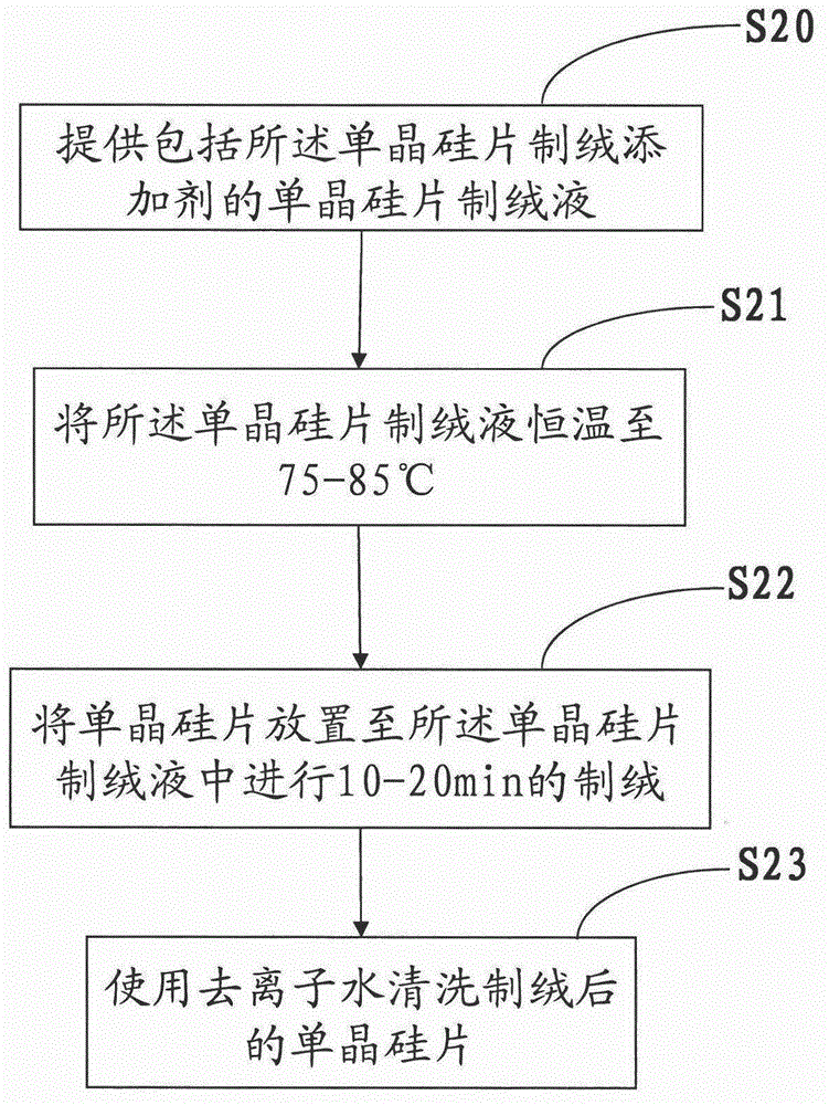
[0026] specific implementation plan

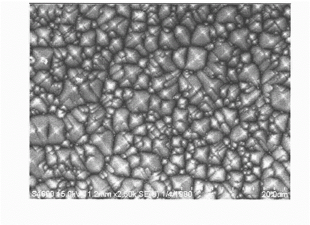
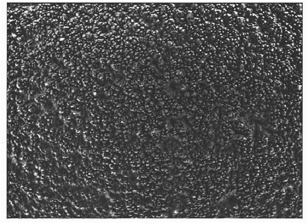
[0027] The purpose and effects of the present invention will be described in detail below in conjunction with specific embodiments and accompanying drawings.

[0028] Monocrystalline silicon wafer texturing additive of the present invention comprises terpineol (C 10 h 18 O), polyethylene glycol ether (), lactic acid (C 3 h 6 o 3 ), sodium acetate (CH 3 COONa) and alkali, the mass percent concentration of described terpineol, polyethylene glycol ether, lactic acid, sodium acetate, alkali is respectively 0.1-3%, 0.3-5%, 0.01-5%, 0.01-5% and 0.1% -2%. The alkali is sodium hydroxide (NaOH) or potassium hydroxide (NaOH) or the like.

[0029] In the first embodiment of the monocrystalline silicon wafer texturing additive of the present invention, the mass percentage concentrations of the terpineol, polyethylene glycol ether, lactic acid, sodium acetate, and sodium hydroxide are respectively 0.5%, 0.3%, 0.05%, 0.1%, and 2.0%.

[0030] In...


PUM


Abstract

The invention provides a monocrystalline silicon wafer texturing additive, a texturing solution and a corresponding texturing method. In the prior art, sodium silicate and the like are taken as monocrystalline silicon wafer texturing additives, a silicon wafer is bad in defoaming performance, and the defoaming effect can be guaranteed only by increasing the amount of a defoaming organic solvent, and thus the manufacturing cost is high and a pyramid texture surface is relatively large and not uniform in density at texturing later period. The monocrystalline silicon wafer texturing additive comprises terpilenol, polyglycol ether, lactic acid, sodium acetate and an alkali. The monocrystalline silicon wafer texturing solution comprises the above monocrystalline silicon wafer texturing additive and a texturing primary liquid, and the texturing primary liquid comprises an alkali, a defoaming organic solvent and deionized water. The monocrystalline silicon wafer texturing method comprises firstly providing the above monocrystalline silicon wafer texturing solution, controlling the texturing solution to have a constant temperature of 75-85 DEG C, placing a monocrystalline silicon wafer into the solution to make texture for 10-20 min, and finally using deionized water to clean the monocrystalline silicon wafer subjected to texturing. According to the technical scheme, the size of the pyramid texture surface can be effectively reduced, the technology stability and consistency are improved, the texture surface density is improved, and the production cost is reduced.

Description

technical field [0001] The invention relates to the field of solar cell manufacturing, in particular to a monocrystalline silicon wafer texturing additive, a texturing liquid and a corresponding texturing method. Background technique [0002] Crystalline silicon solar cells are still the mainstream in the photovoltaic industry. The preparation process of crystalline silicon solar cells includes the following steps: (1) chemical texturing and cleaning; (2) diffusion to prepare PN junctions; (3) etching to remove edges and cleaning ; (4) Preparation of anti-reflection film; (5) Screen printing electrodes and sintering; (6) Battery test sorting. The chemical texturing in the first step above is to form a textured surface on the surface of the silicon wafer and remove the damaged layer formed when the silicon wafer is cut. The monocrystalline silicon wafer usually uses an alkaline etching solution to form a pyramid with a good anti-reflection effect on the surface. Suede, the a...

Claims


Application Information

Patent Timeline
IPC IPC(8): C30B33/10C23F1/32
Inventor 何悦何双权李志刚
Owner 선테크파워컴퍼니리미티드
Why Eureka
Try Eureka