Enhanced graphene waveguide photodetector for integrally-distributed Bragg reflection grating

A distributed Bragg and reflective grating technology, which is applied in semiconductor devices, electrical components, circuits, etc., can solve the problems of low photoresponsivity and achieve the effects of wide spectral range, low insertion loss, and increased light field intensity

Active Publication Date: 2014-07-23
INST OF SEMICONDUCTORS - CHINESE ACAD OF SCI
View PDF3 Cites 31 Cited by
  • Summary
  • Abstract
  • Description
  • Claims
  • Application Information

AI Technical Summary

Problems solved by technology

[0006] The object of the present invention is to provide an enhanced graphene waveguide detector integrating distributed Bragg reflection gratings, which integrates graphene photodetectors with waveguides, resonant cavities, etc., and overcomes the defect of low photoresponsivity

Method used


Image

  • Enhanced graphene waveguide photodetector for integrally-distributed Bragg reflection grating

Examples


Embodiment Construction

[0022] The structure is just an example to make the scheme clearer, and the device involved in the present invention is not limited to the structure shown in the accompanying drawings. In the drawings, for clarity, the thicknesses of the layers and regions are enlarged. It should be considered to strictly reflect the geometric dimensions and the proportional relationship between the various layers.

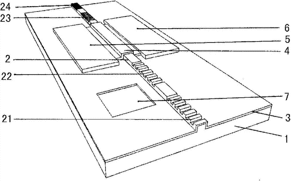
[0023] see figure 1 As shown, the present invention provides a kind of enhanced graphene waveguide detector of integrated distributed Bragg reflection grating, and this photodetector is made on SOI substrate 1, comprises:

[0024] An optical waveguide 2, the optical waveguide 2 is strip-shaped, formed on the longitudinal top of the substrate 1, the optical waveguide 2 includes an input coupling grating 21, a first DBR grating 22, a second DBR grating 23 and an output coupling grating 24, the input coupling grating 21 and the first DBR grating 22 are located on one side of the gra...


PUM

PropertyMeasurementUnit
carrier mobilityaaaaaaaaaa
thicknessaaaaaaaaaa

Abstract

The invention provides an enhanced graphene waveguide photodetector for an integrally-distributed Bragg reflection grating. The photodetector is manufactured on an SOI substrate and comprises an optical waveguide, an insulating transparent thin film, a graphene thin film, a first metal electrode, a second metal electrode and a gate electrode window. The optical waveguide is formed on the substrate in the longitudinal direction. The insulating transparent thin film is evenly manufactured on the substrate and covers the optical waveguide. The graphene thin film is manufactured on the insulating transparent thin film and covers the middle of the strip-shaped optical waveguide. The first metal electrode is provided with a contact end and a strip-shaped electrode end, the contact end of the first metal electrode is manufactured on one side of the insulating transparent thin film, and the electrode end of the first metal electrode is longitudinally manufactured on the graphene thin film. The second metal electrode is provided with a contact end and a strip-shaped electrode end, the contact end of the second metal electrode is manufactured on one side of the insulating transparent thin film, and the electrode end of the second metal electrode is longitudinally manufactured on the graphene thin film. The gate electrode window is formed on the insulating transparent thin film and located on any exposed surface of the insulating transparent thin film. The graphene photodetector is integrated with the waveguide, a resonant cavity and the like, and the defect of low optical responsivity is overcome.

Description

technical field [0001] The invention relates to the technical field of applying graphene to optical communication, optical sensing and optical interconnection, in particular to an enhanced graphene waveguide detector integrating distributed Bragg reflection gratings. Background technique [0002] In future optical communications, integrated, high-speed, and miniaturized photodetectors are essential. Graphene is an emerging two-dimensional material, its fabrication process is compatible with CMOS process, and it is easy to integrate with silicon-based modulators. [0003] Graphene is a two-dimensional crystal composed of carbon atoms on a single-layer honeycomb crystal lattice. The thickness of a single layer is only about 0.335nm, which ensures the miniaturization of photodetectors. Theory shows that graphene will transmit 97.7% of the light in the visible light band, while most of the remaining 2.3% will be absorbed, and only about 0.1% of the light will be reflected. Sin...

Claims


Application Information

Patent Timeline
Patent Type & Authority Applications(China)
IPC IPC(8): H01L31/112H01L31/0232
CPCH01L31/02327H01L31/028H01L31/09
Inventor 王玉冰尹伟红韩勤杨晓红
Owner INST OF SEMICONDUCTORS - CHINESE ACAD OF SCI
Why Eureka
Try Eureka