Piezoresistive electronic skin and preparation method thereof

An electronic skin and piezoresistive technology, applied in the field of sensors, can solve problems such as complex processing technology and device structure, non-transparent and non-flexible limitations, large driving voltage, etc., and achieve high sensitivity, short response time, and low operating voltage. Effect

Active Publication Date: 2014-08-06
SUZHOU INST OF NANO TECH & NANO BIONICS CHINESE ACEDEMY OF SCI
View PDF12 Cites 29 Cited by
  • Summary
  • Abstract
  • Description
  • Claims
  • Application Information

AI Technical Summary

Problems solved by technology

[0003] Although since 2004, some research groups in Japan and the United States have reported electronic skin based on organic field effect transistor type, capacitive type and piezoresistive type, but each has advantages and disadvantages, for example, complex processing technology and device structure, relatively Large driving voltage, low sensitivity, and the use of rigid silicon-based materials make the device non-transparent and non-flexible, which also limits the scope of use of the device.

Method used


Image

  • Piezoresistive electronic skin and preparation method thereof
  • Piezoresistive electronic skin and preparation method thereof
  • Piezoresistive electronic skin and preparation method thereof

Examples


Embodiment Construction

[0037] The present invention will be further described in detail below in conjunction with the accompanying drawings and specific embodiments.

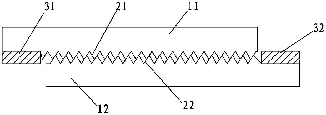
[0038] Please refer to figure 1 , this embodiment discloses a piezoresistive electronic skin, which includes:

[0039] Two flexible substrates 11, 12;

[0040] Two conductive layers 21, 22 are respectively coated on two flexible substrates 11, 12, and the two conductive layers 21, 22 are in contact with each other;

[0041] The two conductive electrodes 31, 32 are in contact with the two conductive layers 21, 22 respectively.

[0042] The at least one flexible substrate is a polydimethylsiloxane film, at least one side of the polydimethylsiloxane film has a micro-nano pattern, and the size of the pattern is between 0.1-500 μm.

[0043] The conductive layers 21 and 22 include a carbon nanotube film, and the carbon nanotube film is mainly composed of a carbon nanotube interweaving network. The light transmittance of the carbon nanot...


PUM

PropertyMeasurementUnit
sizeaaaaaaaaaa
thicknessaaaaaaaaaa
thicknessaaaaaaaaaa

Abstract

The invention provides piezoresistive electronic skin and a preparation method thereof. A carbon nano tube thin film is adopted as an electroconductive layer, and a substrate is made by materials, with micro-nano patterns, like polydimethyl siloxane, polyphenyl dioctyl phthalate ethyl diester, polyvinyl alcohol, polyvinyl formal and polyethylene, so that the substrate is enabled to have the advantages of high flexibility, easiness in bending and the like, and the piezoresistive electronic skin is low in working voltage, small in power consumption, high in flexibility and short in response time. More importantly, the patterned flexible substrate is adopted as a base body, so that sensitivity, of the electronic skin, on outside small acting force is improved greatly.

Description

technical field [0001] The invention relates to the field of sensors, in particular to a piezoresistive electronic skin and a preparation method thereof. Background technique [0002] Robots, as automation devices of artificial intelligence, are more and more integrated into the daily life of human beings, and perform related work instead of human beings in dangerous industries such as high temperature, high pressure, and explosive discharge. The current robot system has achieved many functions such as human vision, hearing and smell through the integration of various sensors. However, how to have a sensitive tactile function like humans has always been one of the challenging problems faced by robotic systems. The birth of electronic skin will bring great changes to the robot system, so that the robot can obtain more information from the external environment. [0003] Although since 2004, some research groups in Japan and the United States have reported electronic skin bas...

Claims


Application Information

Patent Timeline
Patent Type & Authority Applications(China)
IPC IPC(8): A61B5/0205A61B3/00A61B5/11
Inventor 张珽王学文顾杨熊作平李光辉
Owner SUZHOU INST OF NANO TECH & NANO BIONICS CHINESE ACEDEMY OF SCI
Why Eureka
Try Eureka