Method for testing uneven damage to channel of MOS device
A MOS device and channel technology, applied in the field of microelectronics, can solve the problems that the quality of the device cannot meet the use requirements, expensive operation, complexity, etc., and achieve the effect of clear test method, easy data processing, and improved channel quality.
- Summary
- Abstract
- Description
- Claims
- Application Information
AI Technical Summary
Problems solved by technology
Method used
Image
Examples
Embodiment Construction
[0028] The specific implementation manner of the present invention will be described in further detail below in conjunction with the accompanying drawings. The following examples are used to illustrate the present invention, but are not intended to limit the scope of the present invention.
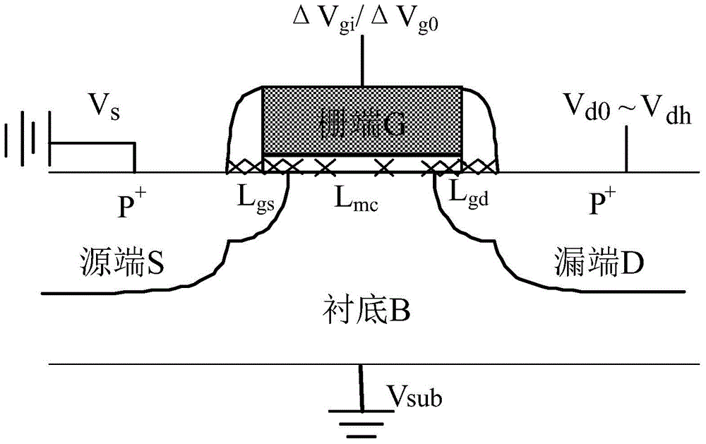
[0029] In this example, a PMOS device with a gate width-to-length ratio W / L of 10 μm / 1 μm and a gate oxide layer thickness of 1.4 nm is selected to test the uneven damage of the channel. The MOS device channel is divided into three regions: the gate-drain overlap region L gd , Gate-source overlap region L gs and the middle channel region L mc , the degree of concentration of damage in different regions is different. The forward test can accurately analyze the gate-drain overlap region L at the channel of the MOS device gd The impact and proportion of the uneven damage on the reliability of the device, and the corresponding reverse test can study the gate-source overlap area L of the MO...
PUM
 Abstract
Description
Claims
Application Information


