Wet etching system and method

A wet etching, wafer technology, applied in the direction of conveyor objects, electrical components, semiconductor/solid device manufacturing, etc., can solve the problem of increased etching difference between the top of the wafer and the bottom of the wafer, and reduce the wet The effect of different etching methods and improving the etching quality

Active Publication Date: 2014-08-13
SHANGHAI INTEGRATED CIRCUIT RES & DEV CENT
View PDF4 Cites 8 Cited by
  • Summary
  • Abstract
  • Description
  • Claims
  • Application Information

AI Technical Summary

Problems solved by technology

The superposition of multiple wet etching differences will inevitably result in a multiplied increase in the etching difference between the top of the wafer and the bottom of the wafer

Method used


Image

  • Wet etching system and method
  • Wet etching system and method
  • Wet etching system and method

Examples


Embodiment 1

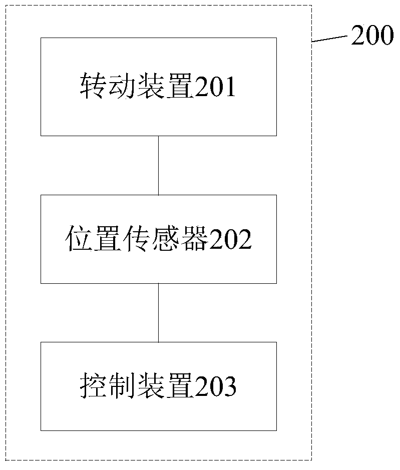
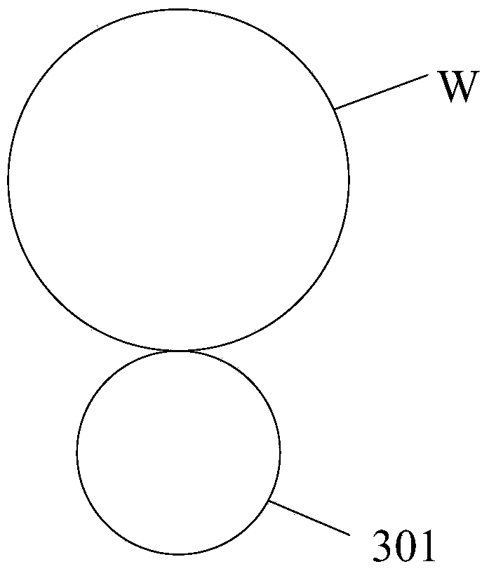
[0047] The following is attached Figure 2-4 As well as specific embodiments, the wet etching chemical solution tank of the present invention will be described in detail. in, figure 2 is a block diagram of the wet etching system of the present invention, image 3 It is a structural schematic diagram of a rotating device in a preferred embodiment of the present invention, Figure 4 It is a structural schematic diagram of a rotating device in another preferred embodiment of the present invention. It should be noted that the drawings are all in a very simplified form, using imprecise scales, and are only used to facilitate and clearly achieve the purpose of assisting in describing the present embodiment.

[0048] see figure 2 , the wet etching system 200 of the present invention includes: a wafer card slot for carrying a plurality of wafers vertically placed in parallel; a chemical solution tank for performing a wet etching process; The card slot is placed in the chemical ...

Embodiment 2

[0060] The following is attached Figure 5 and specific embodiments, the wet etching method of the present invention will be described in detail. in, Figure 5 It is a schematic flow chart of the wet etching method according to Embodiment 2 of the present invention.

[0061] see Figure 5 , the wet etching method of the present invention, adopts above-mentioned wet etching system to operate, specifically comprises the following steps:

[0062] Step S01: the control device controls the manipulator to place the wafer slot carrying a plurality of wafers vertically placed in parallel into the liquid medicine tank;

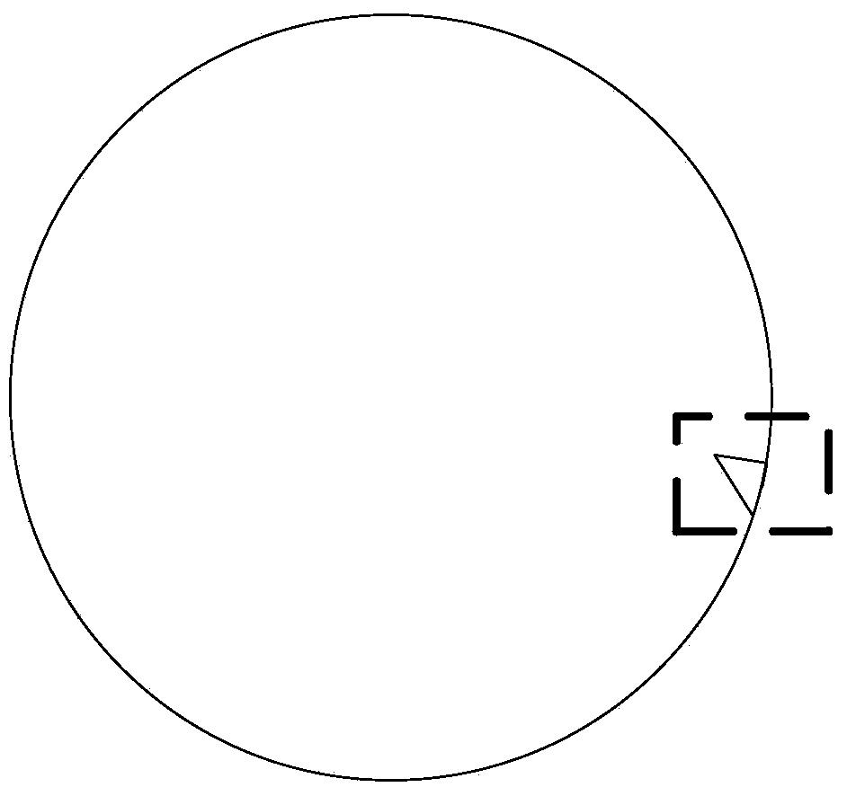
[0063] Specifically, in a preferred embodiment of the present invention, the rotating device is fixed at the bottom of the liquid medicine tank. First, the existing method can be used to align all the wafers at the same position using the V-groove alignment device. ; Then, the wafer card slot is aligned with the wafer from below the wafer and stuck in the wafer car...

Embodiment 3

[0078] The following is attached Image 6 and specific embodiments, the wet etching method of the present invention will be further described in detail. in, Image 6 It is a schematic flowchart of the wet etching method according to the third embodiment of the present invention. In this embodiment, the rotating device includes: a transmission component and a driving component. The difference between the third embodiment and the second embodiment is that the wafer rotation process of the second embodiment is to rotate immediately after entering the chemical liquid tank; the wafer rotation process of the third embodiment is a wet etching process Afterwards, the wafer is spun before leaving the chemical bath.

[0079] Specifically, see Image 6 , the wet etching method in this embodiment includes the following steps:

[0080] Step A01: the control device controls the manipulator to place the wafer slot carrying multiple wafers placed vertically in parallel into the chemical ...


PUM


Abstract

The invention provides a wet etching system. The wet etching system comprises a wafer clamping groove, a solution groove, a manipulator, a control device, a position sensor and a rotating device. When the position sensor detects that wafers are completely immersed in a solution and / or the wafers make contact with the rotating device, a signal is sent to the control device, the control device controls the rotating device to rotate after receiving the signal sent by the position sensor, and the rotating device drives the edges of the wafers to rotate clockwise or counterclockwise; after the edges of the wafers rotate clockwise or counterclockwise by 180 degrees, the control device controls the rotating device to stop rotating. According to the wet etching system, all positions of the surfaces of the wafers can be immersed in the solution for the same time, and therefore the problem that in an existing wet etching method, an etching difference is large because the top and the bottom of a wafer are immersed in a solution for different times is solved, wet etching differences of the surfaces of the wafers are reduced, and etching quality and the quality of a device are improved.

Description

technical field [0001] The invention relates to the technical field of semiconductors, in particular to a wet etching system for improving the wet etching difference on the surface of a wafer, and a method for wet etching the surface of a wafer by using the wet etching system. Background technique [0002] In the field of semiconductor manufacturing process, usually, the edge of the wafer has a small sharp corner, that is, a V-shaped groove (notch), such as figure 1 As shown, it is a schematic diagram of the wafer. The part enclosed by the dotted line represents the notch. The notch is used as a wafer alignment mark. It should be noted that the actual notch is very small. In the figure, the notch is used for clarity scaled up. In many wet etch tools, wafers are processed in batches. After the cassette containing the wafer enters the etching machine, the wafer will be transferred to a notch alignment device. After aligning the notch of all wafers at the same position, the ...

Claims


Application Information

Patent Timeline
IPC IPC(8): H01L21/67H01L21/66H01L21/677H01L21/02
CPCH01L21/02019H01L21/67086H01L21/67259H01L21/68792
Inventor 姚嫦娲
Owner SHANGHAI INTEGRATED CIRCUIT RES & DEV CENT
Why Eureka
Try Eureka