Heterojunction solar cell with selective emitting electrode and manufacturing method thereof

A solar cell and emitter technology, applied in photovoltaic power generation, circuits, electrical components, etc., can solve the problems of high doping concentration, reduced passivation effect, reduced open-circuit voltage and short-circuit current, etc.

Active Publication Date: 2014-08-13
TRINA SOLAR CO LTD
View PDF5 Cites 5 Cited by
  • Summary
  • Abstract
  • Description
  • Claims
  • Application Information

AI Technical Summary

Problems solved by technology

[0002] At present, when using N-type crystalline silicon as a substrate to make heterojunction solar cell devices, the intrinsic type (intrinsic) amorphous silicon film (a-Si:H) is generally used to passivate the upper and lower sides of crystalline silicon (substrate). surface, while adding heavily doped p+-a-Si:H to form the emitter and n+-a-Si:H to form the back field (BSF), but because the uniform emitter requires higher doping concentration and thicker The thickness of the emitter, due to the existence of defects formed by boron atoms in the emitter, the recombination of carriers in the emitter region reduces the passivation effect, resulting in a reduction in the open circuit voltage and short circuit current, which in turn reduces the conversion efficiency of the overall battery

Method used


Image

  • Heterojunction solar cell with selective emitting electrode and manufacturing method thereof
  • Heterojunction solar cell with selective emitting electrode and manufacturing method thereof
  • Heterojunction solar cell with selective emitting electrode and manufacturing method thereof

Examples


Embodiment 1

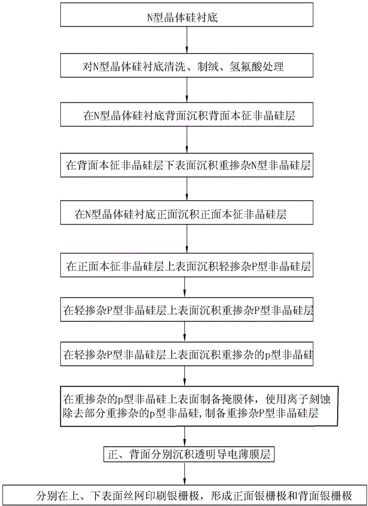
[0023] like figure 1 As shown, a heterojunction solar cell with a selective emitter, which includes:

[0024] An N-type crystalline silicon substrate 1, which has a front side and a back side;

[0025] A front intrinsic amorphous silicon layer 2 deposited on the front surface of the N-type crystalline silicon substrate 1;

[0026] A lightly doped P-type amorphous silicon layer 3 deposited on the upper surface of the front intrinsic amorphous silicon layer 2;

[0027] A front transparent conductive film layer 4, located on the upper surface of the lightly doped P-type amorphous silicon layer 3;

[0028] A front silver grid 5, located on the upper surface of the front transparent conductive film layer 4;

[0029] A heavily doped P-type amorphous silicon layer, used as a selective emitter, is arranged on the contact portion between the front transparent conductive film layer 4 and the lightly doped P-type amorphous silicon layer 3, which has a plurality of heavily doped P-type...

Embodiment 2

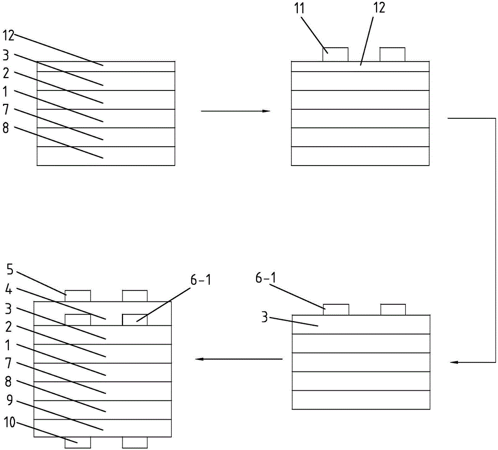
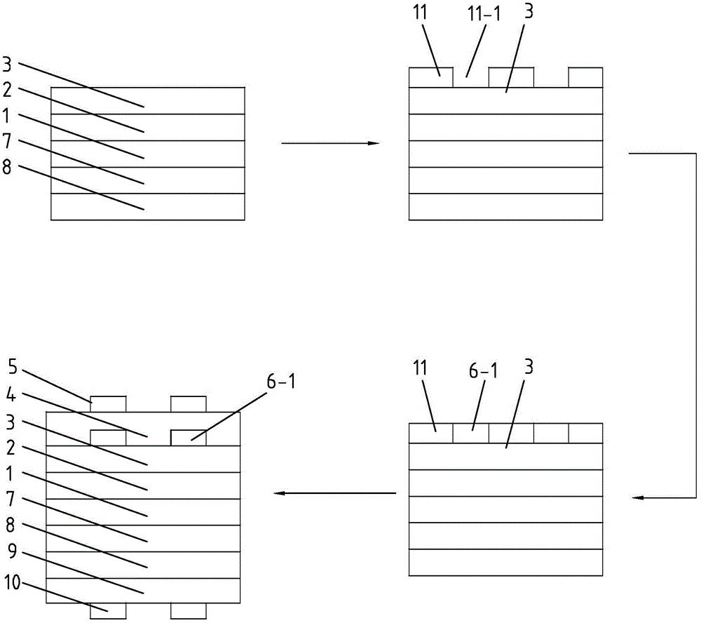
[0037] like image 3 , 4 As shown, the final structure of the heterojunction solar cell with a selective emitter in Example 2 is the same as that of Example 1, the difference is its preparation method, and the preparation method in Example 2 is as follows: N with a thickness of about 200 microns N-type crystalline silicon is cleaned by standard RCA, textured and HF acid dip treatment, and a layer of intrinsic amorphous silicon layer 7 on the back is deposited by PECVD process on the back, with a thickness of 3-15nm, to passivate the N-type crystalline silicon substrate 1 reduce the surface recombination rate, and then deposit a layer of heavily doped n+-a-Si:H, with a typical thickness of 3-20nm, to form a heavily doped N-type amorphous silicon layer 8, on the N-type crystalline silicon lining Deposit a layer of intrinsic amorphous silicon layer 2 on the front side of the bottom 1 through PECVD process, with a thickness of 3-15nm, passivate the front side of the N-type crysta...


PUM


Abstract

The invention discloses a heterojunction solar cell with a selective emitting electrode and a manufacturing method of the heterojunction solar cell. The heterojunction solar cell comprises an N-type crystalline silicon substrate, a front-face intrinsic amorphous silicon layer, a light doped P-type amorphous silicon layer, a front-face transparent conducting film layer, a front-face silver grid electrode, a heavy doped P-type amorphous silicon layer, a back-face intrinsic amorphous silicon layer, a heavy doped N-type amorphous silicon layer, a back-face transparent conducting film layer and a back-face silver grid electrode, and the N-type crystalline silicon substrate is provided with a front face and a back face. The heavy doped P-type amorphous silicon layer is adopted as the selective emitting electrode, is arranged at the contact position of the front-face transparent conducting film layer and the light doped P-type amorphous silicon layer and is provided with a plurality of heavy doped P-type amorphous silicon monomers, and the heavy doped P-type amorphous silicon monomers correspond to grid wires of the front-face silver grid electrode one to one and are located under the corresponding grid wires respectively. The heavy doped N-type amorphous silicon layer is deposited on the lower surface of the back-face intrinsic amorphous silicon layer. According to the solar cell and the manufacturing method, recombination of current carriers can be reduced, absorption of the emitting electrode on the current carriers is reduced, and therefore open-circuit voltages and short-circuit currents are improved, and the efficiency of the heterojunction cell is improved.

Description

technical field [0001] The invention relates to a heterojunction solar cell with a selective emitter and a preparation method thereof, belonging to the technical field of heterojunction solar cells. Background technique [0002] At present, when using N-type crystalline silicon as a substrate to make heterojunction solar cell devices, the intrinsic type (intrinsic) amorphous silicon film (a-Si:H) is generally used to passivate the upper and lower sides of crystalline silicon (substrate). surface, while adding heavily doped p+-a-Si:H to form the emitter and n+-a-Si:H to form the back field (BSF), but because the uniform emitter requires higher doping concentration and thicker The thickness of the emitter, due to the existence of defects formed by boron atoms in the emitter, the recombination of carriers in the emitter region reduces the passivation effect, resulting in a reduction in the open circuit voltage and short circuit current, which in turn reduces the conversion effi...

Claims


Application Information

Patent Timeline
Patent Type & Authority Applications(China)
IPC IPC(8): H01L31/0747H01L31/0352H01L31/20
CPCY02E10/50H01L31/035245H01L31/0747H01L31/202Y02P70/50
Inventor 包健
Owner TRINA SOLAR CO LTD
Why Eureka
Try Eureka