
Scribing method

A scribing and scribing technology, which is applied in laser welding equipment, electrical components, circuits, etc., can solve problems such as insufficient ablation zone width, fragmentation of LED epitaxial wafers, excessive stress, etc., to ensure appearance yield and reduce fragmentation rate effect

Inactive Publication Date: 2014-08-20
HC SEMITEK SUZHOU
View PDF6 Cites 0 Cited by
  • Summary
  • Abstract
  • Description
  • Claims
  • Application Information

AI Technical Summary

Problems solved by technology

[0003] In the process of realizing the present invention, the inventors have found that the prior art has at least the following problems: if the laser power is high during scribing, the stress on the scribing ablation area (scribing lane) on the substrate will be too large, and the substrate will be damaged before slicing. The bottom will crack naturally along the scribing path, causing the LED epitaxial wafer to become fragments; if the laser power is low during scribing, the width of the scribing and ablation area on the substrate will not be enough, which will lead to poor appearance of the LED chip after slicing (including cracks) chaos and twins)
However, the laser power range suitable for scribing is very small and it is difficult to adjust it in place

Method used


Image

  • Scribing method
  • Scribing method
  • Scribing method

Examples


Embodiment 1

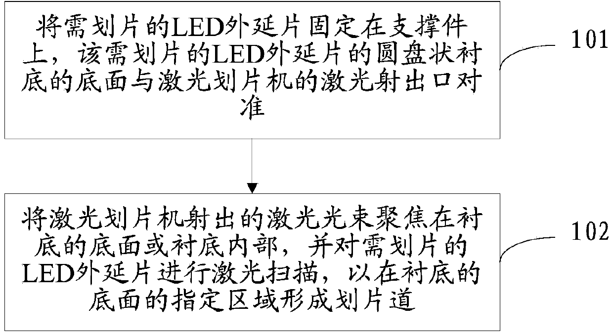
[0044] The embodiment of the present invention provides a scribing method, see figure 1 , the method includes:

[0045] Step 101: Fix the LED epitaxial wafer to be diced on the support member, and align the bottom surface of the disk-shaped substrate of the LED epitaxial wafer to be diced with the laser injection port of the laser scribing machine.

[0046] As an optional mode of this embodiment, the LED epitaxial wafer to be diced can be fixed on the support in such a way that the bottom surface of the disc-shaped substrate of the LED epitaxial wafer is horizontally upward, and the support is located on the laser scribing machine. Right below the laser exit.

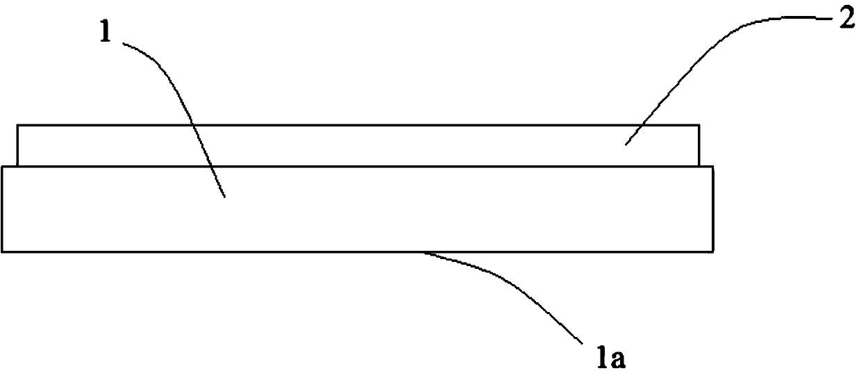
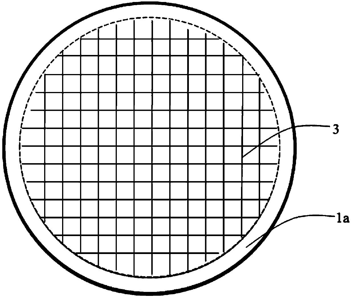
[0047] see figure 2, the LED epitaxial wafer is composed of a substrate 1 and an LED chip array 2 grown on the substrate 1 . The substrate 1 is disc-shaped, and the material of the substrate 1 can be sapphire or silicon carbide. In the embodiment of the present invention, the bottom surface 1a of the substrate 1 re...

Embodiment 2

[0054] The embodiment of the present invention provides a scribing method, see Figure 4 , the method includes:

[0055] Step 201: Fix the LED epitaxial wafer to be diced on the support, and align the bottom surface of the disk-shaped substrate of the LED epitaxial wafer to be diced with the laser injection port of the laser scribing machine.

[0056] Wherein, the supporting member may be a platform or a bracket.

[0057] Optionally, a protective film may be provided between the LED epitaxial wafer to be diced and the support.

[0058] Step 202: placing a preset tooling on the bottom surface of the substrate, and the preset tooling will cover a designated area of ​​the bottom surface of the substrate.

[0059] Wherein, the specified area is a concentric circle of the bottom surface of the substrate, and the radius of the specified area is smaller than the radius of the bottom surface of the substrate.

[0060] Optionally, the preset tooling may be in the shape of a hollow r...

Embodiment 3

[0074] The embodiment of the present invention provides a scribing method, see Figure 5 , the method includes:

[0075] Step 301: Fix the LED epitaxial wafer to be diced on the support, and align the bottom surface of the disc-shaped substrate of the LED epitaxial wafer to be diced with the laser injection port of the laser scribing machine.

[0076] This step 301 is the same as step 201, and will not be repeated here.

[0077] Step 302: Start the laser scribing machine, and focus the laser beam emitted by the laser scribing machine on the bottom surface of the substrate or inside the substrate, and the laser beam forms spot-like spots on the substrate.

[0078] Step 302 is the same as step 203, and will not be repeated here.

[0079] Step 303 : moving the laser outlet so that the dot-like spots form a plurality of first scribing lanes parallel to each other in a designated area on the bottom surface of the substrate.

[0080] Wherein, the moving direction of the laser inj...


PUM


Abstract

The invention discloses a scribing method, and belongs to the field of an LED. The method comprises: fixing an LED epitaxial wafer needing to be scribed on a support member, the bottom surface of the discoid substrate of the LED epitaxial wafer needing to be scribed being aligned with the laser emitting port of a laser scribing machine; and focusing laser beams emitted by the laser scribing machine to the bottom surface of the substrate or inside the substrate, performing laser scanning on the LED epitaxial wafer needing to be scribed, and forming a scribing channel in a specific area of the bottom surface of the substrate, the specific area being a concentric circle of the bottom surface of the substrate and the radius of the specific area being smaller than the radius of the bottom surface of the substrate. The scribing method reduces the fragmentation rate of the LED epitaxial wafer before splinting, and ensures the appearance yield rate of a single LED chip obtained after splinting of an LED chip array.

Description

technical field [0001] The invention relates to the field of light emitting diodes, in particular to a scribing method. Background technique [0002] The manufacturing process of a light-emitting diode (Light-Emitting Diode, referred to as LED) includes, first, manufacturing an LED epitaxial wafer, and the LED epitaxial wafer is composed of a substrate and an array of LED chips grown on the substrate. Secondly, the bottom surface of the substrate of the LED epitaxial wafer is scribed by laser scanning scribing, and scribing lanes are arranged on the entire area of ​​the bottom surface of the substrate. Finally, the diced LED epitaxial wafer is split, so that the LED chip array on the LED epitaxial wafer is divided into individual LED chips along the dicing lane. [0003] In the process of realizing the present invention, the inventors have found that the prior art has at least the following problems: if the laser power is high during scribing, the stress on the scribing abl...

Claims


Application Information

Patent Timeline
IPC IPC(8): H01L21/78B23K26/38
CPCH01L21/78
Inventor 刘源张超王超群
Owner HC SEMITEK SUZHOU
Learn More