Chip for two-way voltage regulator diode DB3 and manufacturing technique thereof

A technology of two-way voltage stabilization and production process, which is applied in the photoengraving process, optics, instruments and other directions of the pattern surface, which can solve the problem of high corrosion debris rate in deep mesa grooves, insufficient high temperature rebound voltage, and insufficient breakdown voltage. and other problems, to achieve the effect of improving voltage resistance stability, reducing high temperature power consumption, and improving stability

Active Publication Date: 2011-06-01
TIANJIN ZHONGHUAN SEMICON CO LTD
View PDF3 Cites 15 Cited by
  • Summary
  • Abstract
  • Description
  • Claims
  • Application Information

AI Technical Summary

Problems solved by technology

The existing problems in the prior art include: 1), the breakdown voltage is not stable enough, high temperature and long time work will produce backflow, which will affect the start-up
2) The high temperature rebound voltage is not large enough, which affects the triggering ability
3) High rate of corrosion fragments in deep mesa grooves

Method used


Image

  • Chip for two-way voltage regulator diode DB3 and manufacturing technique thereof
  • Chip for two-way voltage regulator diode DB3 and manufacturing technique thereof
  • Chip for two-way voltage regulator diode DB3 and manufacturing technique thereof

Examples


Embodiment Construction

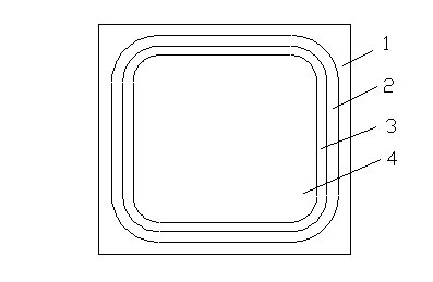
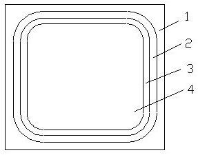
[0023] Such as figure 1 The chip structure of the bidirectional Zener diode DB3 shown is N + PN + type. The chip sections are chip 1 of DB3, mesa groove 2, glass layer 3, and metal surface 4 in sequence.

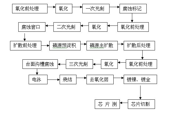
[0024] Such as figure 2 The production process of the shown bidirectional voltage regulator diode DB3 is as follows:

[0025] 1) Pre-oxidation treatment: chemically treat the surface of silicon wafers through acid, alkali, deionized water and other processes.

[0026] 2) Oxidation: Clean the original silicon wafer, grow an oxide layer in an oxidation furnace at 1100-1200 ° C as a mask, and prepare to open windows and trenches;

[0027] 3) Three photolithography: the oxidized silicon wafer is coated with glue, photolithographic mark, photolithographic window, photolithographic table top, exposure, development, deoxidation layer and other processes, and the marking, window, and table top graphics are engraved.

[0028] 4) Pre-diffusion treatment: chemically treat the s...


PUM


Abstract

The invention relates to a manufacturing technique of a chip for a two-way voltage regulator diode DB3, wherein the two-way voltage regulator diode DB3 is a symmetrical diode with the structure of N<+> PN<+>. The resilience voltage is increased due to the adoption of a triple photolithographic process, the trigger capacity of the two-way voltage regulator diode is improved; due to the application of shallow mesa or trench etching, the fragmentation rate is reduced; and glass is passivated due to the adoption of an electrophoretic process, the withstand voltage stability and reliability of the two-way voltage regulator diode are improved. The manufacture technique of the chip for the two-way voltage regulator diode has the advantages of improving the breakdown voltage stability of the two-way voltage regulator diode DB3, enhancing the trigger capacity of the diode, reducing the high-temperature power consumption, prolonging the service life of the diode, and simultaneously improving the qualification rate.

Description

technical field [0001] The invention relates to the technical field of crystal diode chip production, in particular to a chip and production process of a bidirectional voltage stabilizing diode DB3, which uses liquid source diffusion, multiple photolithography, shallow trench corrosion, and electrophoresis to improve product performance. Background technique [0002] At present, most of the bidirectional voltage regulator DB3 chips made in the industry use a production process such as a photolithography process, deep mesa groove corrosion, and glass passivation by knife scraping. The existing problems in the prior art include: 1), the breakdown voltage is not stable enough, high temperature and long time work will produce backflow, which will affect the start-up. 2) The high temperature rebound voltage is not large enough, which affects the triggering ability. 3) The corrosion debris rate of deep mesa grooves is high. Contents of the invention [0003] The purpose of the...

Claims


Application Information

Patent Timeline
Patent Type & Authority Applications(China)
IPC IPC(8): H01L21/329H01L29/861G03F7/00H01L21/311
Inventor 刘长蔚王军明初亚东宋进虎徐长坡崔俊发范玉丰邢立勋
Owner TIANJIN ZHONGHUAN SEMICON CO LTD
Why Eureka
Try Eureka