Semiconductor device and method for producing same

A manufacturing method, a semiconductor technology, applied in the direction of semiconductor/solid-state device manufacturing, semiconductor devices, transistors, etc., can solve the problem of carrier mobility reduction, achieve low-cost manufacturing methods, improve the increase of on-resistance, stabilize and manufacture The effect of the method

Active Publication Date: 2014-08-20
FUJI ELECTRIC CO LTD
View PDF9 Cites 12 Cited by
  • Summary
  • Abstract
  • Description
  • Claims
  • Application Information

AI Technical Summary

Problems solved by technology

In addition, Patent Document 5 describes that the reduction in carrier mobili

Method used


Image

  • Semiconductor device and method for producing same
  • Semiconductor device and method for producing same
  • Semiconductor device and method for producing same

Examples


Embodiment 1

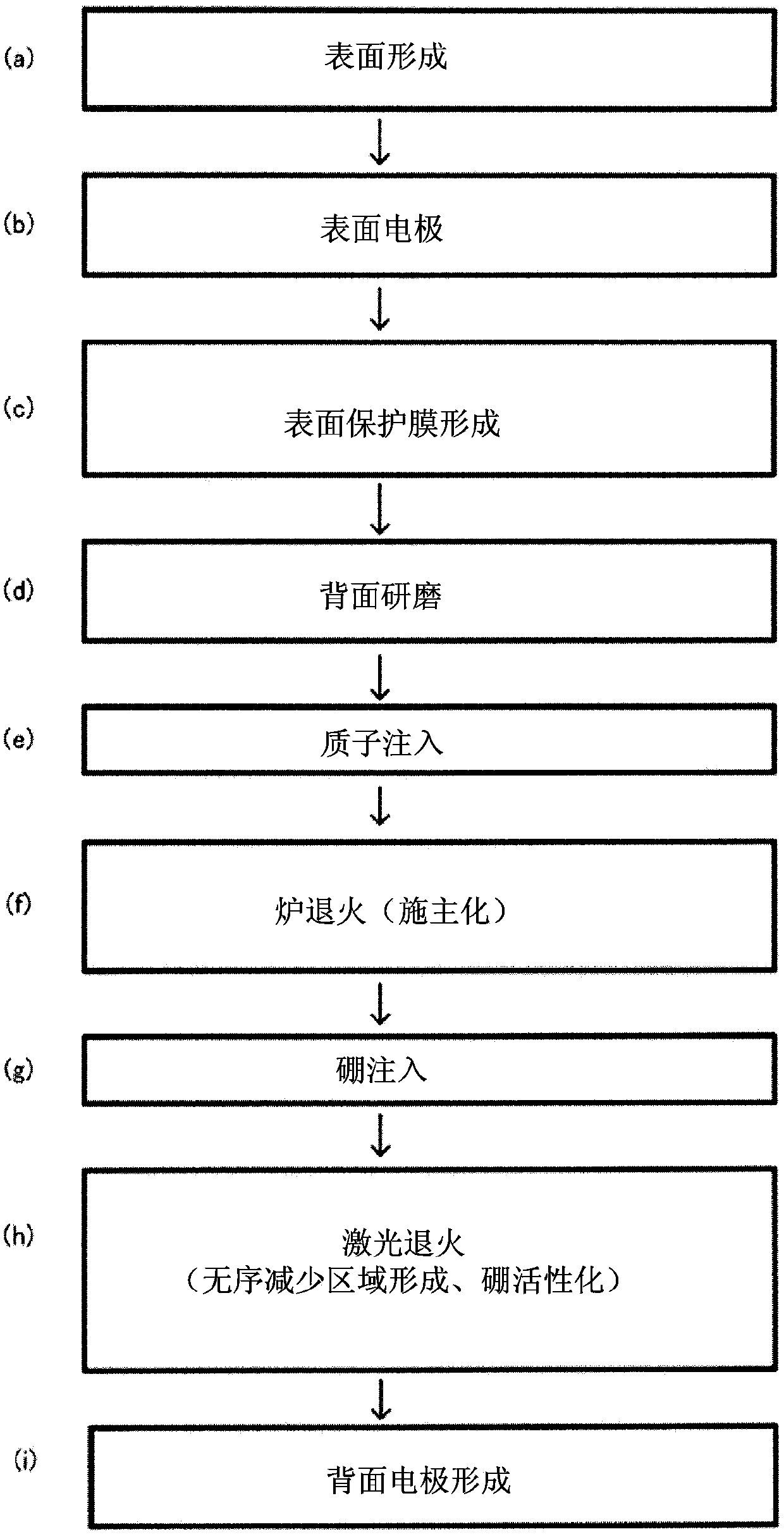
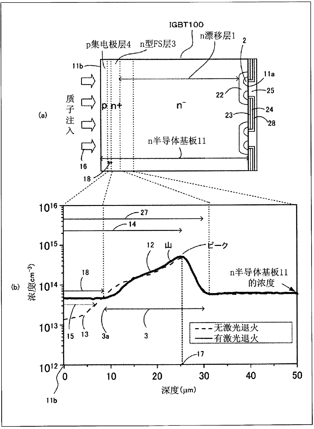
[0057] figure 1 It is a process flow chart showing the manufacturing method of the semiconductor device (IGBT100) of Example 1 of this invention. image 3 is used figure 1 The cross-sectional view (a) of the main part of the IGBT100 produced in the process flow of FIG. refer to figure 1 process flow and image 3 (a) is a cross-sectional view of main parts to describe the method of manufacturing the semiconductor device according to the first embodiment of the present invention.

[0058] First, in figure 1 In the surface forming step of (a), on one main surface (surface 11a) of n semiconductor substrate (wafer) 11, p base layer 22, n emitter layer 2, gate insulating film 23, gate electrode 24, and interlayer insulating film are formed. MOS gate structure composed of film 28 and so on. Wherein, the n-emitting layer 2 is formed in the p-base layer 22 . The configuration of the MOS gate structure will be described later.

[0059] Next, at figure 1 In the surface elec...

Embodiment 2

[0083] The semiconductor device of Example 2 will be described. Figure 4 It is a process flow diagram showing a method of manufacturing a semiconductor device according to Embodiment 2 of the present invention.

[0084] The difference from Example 1 is that after proton implantation, boron implantation ( Figure 4 (e) process), followed by laser annealing ( Figure 4 (f) process) and subsequent furnace annealing treatment ( Figure 4 (g) process). At this time, in the previous laser annealing process, the protons generated in the proton implantation 16 pass through the region 14 to form the n-type disorder-reducing region 18 while activating boron to form the p-collector layer 4 . In addition, in the furnace annealing treatment performed in the subsequent step, protons are donated to form the n-type field stop layer 3 . Also in this case, as in Example 1, by combining the laser annealing treatment and the furnace annealing treatment, the n-type disorder-reduced region 18 ...

Embodiment 3

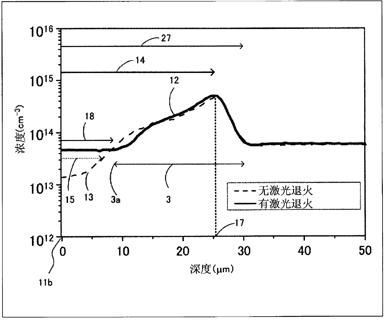
[0088] The semiconductor device of the third embodiment will be described. In Example 3, one or more n-type intermediate layers 27 consisting of a pair of n-type field stop layer 3 and n-type disorder reducing region 18 are formed, for example, an IGBT in which three are formed as in this example. Figure 5 It is a cross-sectional view (a) of a main part of a semiconductor device (IGBT100) according to Example 3 of the present invention and a graph of a carrier concentration curve (b) near the n-type field stop layer 3 . By forming a plurality of n-type intermediate layers 27 in this way, it is possible to relax the diffusion of the depletion layer at the time of turning off, and suppress the oscillation phenomenon at the time of switching (at the time of turning off).


PUM


Abstract

A method of producing a seminconductor device is disclosed in which, after proton implantation is performed, a hydrogen-induced donor is formed by a furnace annealing process to form an n-type field stop layer. A disorder generated in a proton passage region is reduced by a laser annealing process to form an n-type disorder reduction region. As such, the n-type field stop layer and the n-type disorder reduction region are formed by the proton implantation. Therefore, it is possible to provide a stable and inexpensive semiconductor device which has low conduction resistance and can improve electrical characteristics, such as a leakage current, and a method for producing the semiconductor device.

Description

technical field [0001] The present invention relates to semiconductor devices such as diodes and IGBTs (Insulated Gate Bipolar Transistors) having FS (Field Stop) layers, and their manufacturing methods. Background technique [0002] As semiconductor devices for electric power, there are diodes and / or IGBTs having a withstand voltage of 400V, 600V, 1200V, 1700V, 3300V or higher. They can be used in power conversion devices such as converters and / or inverters. For power semiconductor devices, good electrical characteristics such as low loss, high efficiency, and high damage resistance, and low cost are required. [0003] As a method of manufacturing the power semiconductor device, the following method has been proposed. First, a diffusion region and / or a MOS structure and the like are formed on the surface side of the semiconductor substrate. Next, after grinding the back side to thin the semiconductor substrate, proton implantation and heat treatment are performed from th...

Claims


Application Information

Patent Timeline
IPC IPC(8): H01L29/739H01L21/336H01L29/78
CPCH01L29/49H01L29/7395H01L29/0834H01L29/66333H01L29/36H01L29/0646H01L21/268H01L21/324H01L21/26506H01L21/26513H01L29/0615H01L29/0804H01L29/0821H01L29/1004H01L29/1095H01L29/32H01L29/41708H01L29/6609H01L29/861
Inventor 宫崎正行吉村尚泷下博栗林秀直
Owner FUJI ELECTRIC CO LTD
Why Eureka
Try Eureka