A light-emitting diode epitaxial wafer and its manufacturing method
A technology of light-emitting diodes and epitaxial wafers, which is applied in the direction of electrical components, circuits, semiconductor devices, etc., can solve the problems of damaging the activity of multi-quantum well layers, reducing the luminous efficiency of epitaxial wafers, and affecting the hole injection efficiency, so as to reduce difficulty and improve Crystal quality, effect of suppressing electron overflow
- Summary
- Abstract
- Description
- Claims
- Application Information
AI Technical Summary
Problems solved by technology
Method used
Image
Examples
Embodiment 1
[0033] An embodiment of the present invention provides a light emitting diode epitaxial wafer, see figure 1 , the epitaxial wafer includes: a substrate 11, a nucleation layer 12 growing upward on the substrate 11, an undoped GaN layer 14, an n-type layer 15, a multiple quantum well layer 16, and a first p-type GaN layer 171 , the second p-type GaN layer 172 , the electron blocking layer 18 and the p-type layer 19 . The thickness of the electron blocking layer 18 is 50-150nm, the growth temperature of the first p-type GaN layer 171 is 600-800°C, and the growth pressure is 400-800Torr, the growth temperature of the second p-type GaN layer 172 is 800-1000°C, The growth pressure is 50-500 Torr.
[0034] Specifically, the thicknesses of the first p-type GaN layer 171 and the second p-type GaN layer 172 are both 10-50 nm. If the thickness is less than 10nm, the effects of the first p-type GaN layer 171 and the second p-type GaN layer 172 will be affected, and if the thickness is g...
Embodiment 2
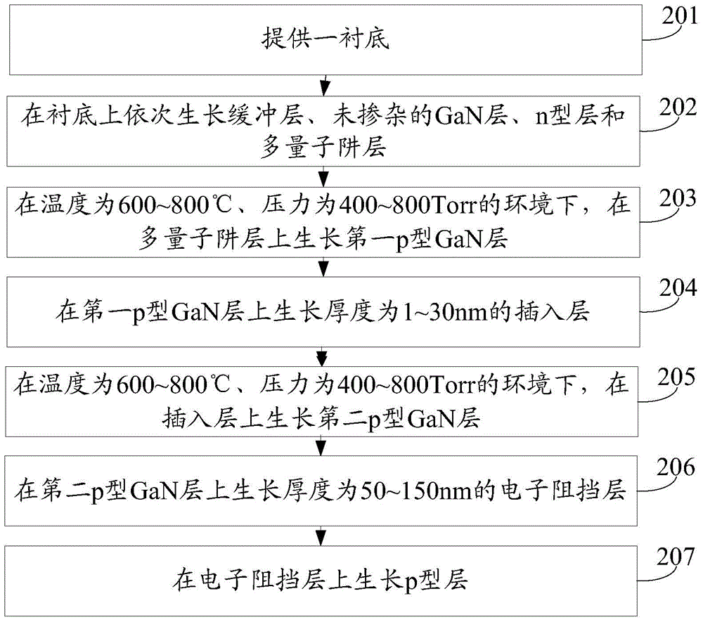
[0062] An embodiment of the present invention provides a method for manufacturing a light-emitting diode epitaxial wafer, see figure 2 , the method includes:
[0063] Step 201: Provide a substrate.
[0064] Specifically, the substrate may be a sapphire substrate.
[0065] Step 202: growing a nucleation layer, an undoped GaN layer, an n-type layer and a multi-quantum well layer sequentially on the substrate.
[0066] Step 203: growing a first p-type GaN layer on the multi-quantum well layer in an environment with a temperature of 600-800° C. and a pressure of 400-800 Torr.
[0067] Step 204: growing an insertion layer with a thickness of 1-30 nm on the first p-type GaN layer.
[0068] Specifically, the thickness of the first p-type GaN layer is 10-50 nm.
[0069] The insertion layer has a periodic structure, each period includes an InGaN layer and an AlInGaN layer, and the Al component content of the AlInGaN layer in each periodic structure of the insertion layer is 1.1-1....
PUM
 Abstract
Description
Claims
Application Information

