Light emitting diode epitaxial wafer and manufacturing method thereof

A technology of light-emitting diodes and epitaxial wafers, applied in electrical components, circuits, semiconductor devices, etc., can solve problems such as increasing difficulty, damaging the activity of multiple quantum well layers, and reducing the luminous efficiency of epitaxial wafers.

Active Publication Date: 2014-08-27
HC SEMITEK SUZHOU
View PDF5 Cites 9 Cited by
  • Summary
  • Abstract
  • Description
  • Claims
  • Application Information

AI Technical Summary

Problems solved by technology

[0005] While the electron blocking layer reduces the electron overflow phenomenon, it also makes it more difficult for holes to transition to the multi-quantum well layer, which affec...

Method used


Image

  • Light emitting diode epitaxial wafer and manufacturing method thereof
  • Light emitting diode epitaxial wafer and manufacturing method thereof

Examples


Embodiment 1

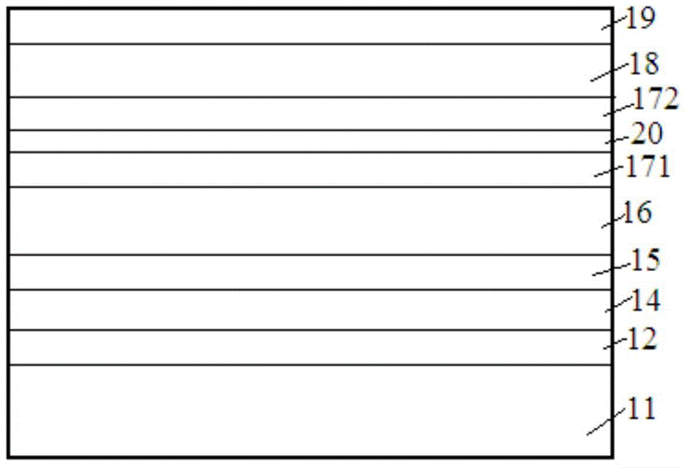
[0033] An embodiment of the present invention provides a light emitting diode epitaxial wafer, see figure 1 , the epitaxial wafer includes: a substrate 11, a nucleation layer 12 growing upward on the substrate 11, an undoped GaN layer 14, an n-type layer 15, a multiple quantum well layer 16, and a first p-type GaN layer 171 , the second p-type GaN layer 172 , the electron blocking layer 18 and the p-type layer 19 . The thickness of the electron blocking layer 18 is 50-150nm, the growth temperature of the first p-type GaN layer 171 is 600-800°C, and the growth pressure is 400-800Torr, the growth temperature of the second p-type GaN layer 172 is 800-1000°C, The growth pressure is 50-500 Torr.

[0034] Specifically, the thicknesses of the first p-type GaN layer 171 and the second p-type GaN layer 172 are both 10-50 nm. If the thickness is less than 10nm, the effects of the first p-type GaN layer 171 and the second p-type GaN layer 172 will be affected, and if the thickness is g...

Embodiment 2

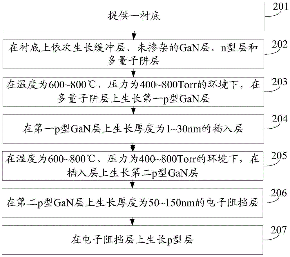
[0062] An embodiment of the present invention provides a method for manufacturing a light-emitting diode epitaxial wafer, see figure 2 , the method includes:

[0063] Step 201: Provide a substrate.

[0064] Specifically, the substrate may be a sapphire substrate.

[0065] Step 202: growing a nucleation layer, an undoped GaN layer, an n-type layer and a multi-quantum well layer sequentially on the substrate.

[0066] Step 203: growing a first p-type GaN layer on the multi-quantum well layer in an environment with a temperature of 600-800° C. and a pressure of 400-800 Torr.

[0067] Step 204: growing an insertion layer with a thickness of 1-30 nm on the first p-type GaN layer.

[0068] Specifically, the thickness of the first p-type GaN layer is 10-50 nm.

[0069] The insertion layer has a periodic structure, each period includes an InGaN layer and an AlInGaN layer, and the Al component content of the AlInGaN layer in each periodic structure of the insertion layer is 1.1-1....


PUM

PropertyMeasurementUnit
Thicknessaaaaaaaaaa
Growth temperatureaaaaaaaaaa
Thicknessaaaaaaaaaa

Abstract

The invention discloses a light emitting diode epitaxial wafer and a manufacturing method of the light emitting diode epitaxial wafer, and belongs to the technical field of semiconductors. The epitaxial wafer comprises a substrate, a nucleating layer, a buffer layer, an undoped GaN layer, an n-type layer, a multiple-quantum-well layer, a first p-type GaN layer, a second p-type GaN layer, an electron barrier layer and a p-type layer, wherein the nucleating layer, the buffer layer, the undoped GaN layer, the n-type layer, the multiple-quantum-well layer, the first p-type GaN layer, the second p-type GaN layer, the electron barrier layer and the p-type layer grow upwards on the substrate. The thickness of the electron barrier layer ranges from 50 nm to 150 nm, the growth temperature of the first p-type GaN layer ranges from 600 DEG C to 800 DEG C, the growth pressure of the first p-type GaN layer ranges from 400 Torr to 800 Torr, the growth temperature of the second p-type GaN layer ranges from 800 DEG C to 1000 DEG C, the growth pressure of the second p-type GaN layer ranges from 50 Torr to 500 Torr. The first p-type GaN layer growing under high pressure and low temperature is arranged, and a hole injection channel is provided, so that hole injection efficiency is improved; through the second p-type GaN layer growing under low pressure and high temperature, crystalline quality is improved, the thickness of the electron barrier layer is limited, and hole injection efficiency is improved.

Description

technical field [0001] The invention relates to the technical field of semiconductors, in particular to a light-emitting diode epitaxial wafer and a manufacturing method thereof. Background technique [0002] GaN (gallium nitride) is a typical representative of the third-generation wide-bandgap semiconductor materials. Its excellent high thermal conductivity, high temperature resistance, acid and alkali resistance, and high hardness make it widely used in blue, green, and UV LEDs. The core component of a GaN-based light-emitting diode is a chip, which includes an epitaxial wafer and electrodes on the epitaxial wafer. [0003] A GaN-based light-emitting diode epitaxial wafer generally includes a substrate, and a buffer layer, an undoped GaN layer, an n-type layer, a multi-quantum well layer and a p-type layer that are sequentially grown upward on the substrate. Since the electron mobility of the n-type layer is relatively high, it is easy to cause electron overflow. In orde...

Claims


Application Information

Patent Timeline
IPC IPC(8): H01L33/32H01L33/02H01L33/04
CPCH01L33/007H01L33/025H01L33/06H01L33/14H01L33/145H01L33/32
Inventor 郭炳磊王群胡加辉童吉楚陶章峰魏世祯
Owner HC SEMITEK SUZHOU
Why Eureka
Try Eureka