Transistors and methods of forming them

A technology of transistors and semiconductors, applied in the fields of semiconductor devices, semiconductor/solid-state device manufacturing, electrical components, etc., can solve the problems that transistors cannot meet, limit the application range of transistors, complex technical requirements, etc., and achieve the effect of size reduction

Active Publication Date: 2016-08-31
SEMICON MFG INT (SHANGHAI) CORP
View PDF5 Cites 0 Cited by
  • Summary
  • Abstract
  • Description
  • Claims
  • Application Information

AI Technical Summary

Problems solved by technology

[0006] However, in the prior art, the threshold voltage of the channel region of the transistor from the source region to the drain region is the same, which makes the transistor unable to meet more complex technical requirements and limits the application range of the transistor

Method used


Image

  • Transistors and methods of forming them
  • Transistors and methods of forming them
  • Transistors and methods of forming them

Examples


no. 1 example

[0043] Figure 2 to Figure 9 is a schematic cross-sectional structure diagram of the formation process of the transistor described in the first embodiment of the present invention.

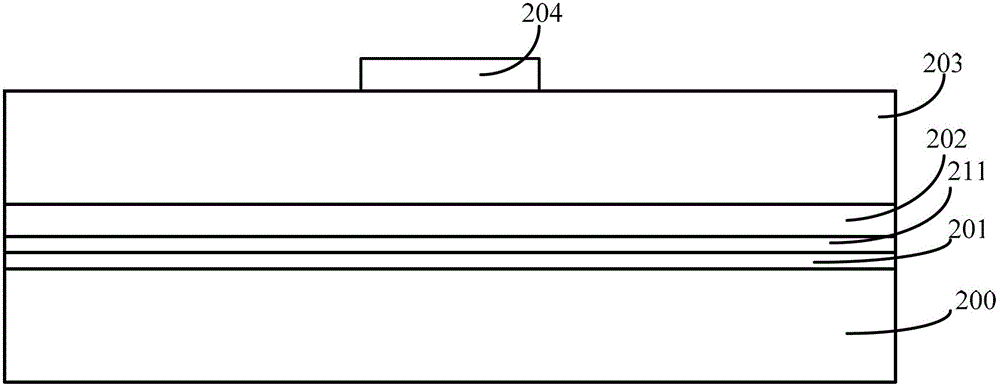
[0044] Please refer to figure 2 , providing a semiconductor substrate 200, forming a gate dielectric film 201 on the surface of the semiconductor substrate 200; forming a first work function film 202 on the surface of the gate dielectric layer film 201; forming a dummy film 202 on the surface of the first work function film 202 A gate film 203 ; a sacrificial layer 204 is formed on the surface of the dummy gate film 203 .

[0045] The semiconductor substrate 200 is used to provide a working platform for subsequent processes; the semiconductor substrate 200 is a silicon substrate, a silicon-germanium substrate, a silicon carbide substrate, a silicon-on-insulator (SOI) substrate, a germanium-on-insulator (GOI) ) substrate, glass substrate or III-V compound substrate (such as gallium arsenide, etc...

no. 2 example

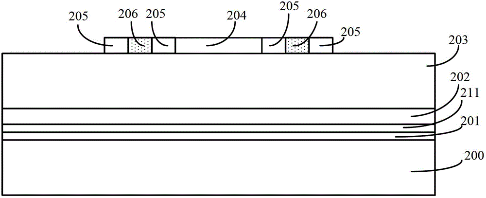
[0086] The difference between the second embodiment and the first embodiment is that in the first embodiment Figure 5 On the basis of removing the second mask layer, and retaining the first mask layer as a mask for etching the first work function layer, the details are as follows.

[0087] exist Figure 5 basis, please refer to Figure 10 , after forming the dielectric layer 207, remove the second mask layer 205 (such as Figure 5 shown); after removing the second mask layer 205, the dummy gate layer 203a and the first work function layer 202a are etched using the dielectric layer 207 and the remaining first mask layer 206 as masks.

[0088] In this embodiment, the second mask layer 205 is removed, and the first mask layer 206 is retained, and then the regions on both sides of the first work function layer 202a can be etched away, and the middle region of the first work function layer 202a is retained; Subsequent formation of the second work function layer can make the wor...


PUM


Abstract

A transistor and a forming method thereof are provided; the forming method of the transistor comprises the following steps: forming a gate medium film, a first work function film, a dummy grid film and a sacrificial layer on a surface of a semiconductor substrate; forming a mask film structure on a surface of the dummy grid film on two sides of the sacrificial layer; removing the sacrificial layer, using the mask film structure as a mask to etch the dummy grid film, the first work function film and the gate medium film until the semiconductor substrate is exposed, thereby forming a gate medium layer, a first work function layer and a dummy grid layer; removing partial mask film structure so as to expose partial surface of the dummy grid layer; using remained mask film structure as the mask to etch the dummy grid layer and the fist work function layer until the gate medium layer is exposed; removing the dummy grid layer and the mask film structure so as to form an opening; forming a second work function layer and a grid electrode layer on a surface of side walls and a bottom portion of the opening, and the work function of the second work function layer is different from that of the first work function layer. By using the method, the performance of the transistor can be improved.

Description

technical field [0001] The invention relates to the technical field of semiconductor manufacturing, in particular to a transistor and a forming method thereof. Background technique [0002] With the rapid development of integrated circuit manufacturing technology, the size of semiconductor devices in integrated circuits, especially MOS (Metal Oxide Semiconductor, metal-oxide-semiconductor) devices, has been continuously reduced to meet the miniaturization and development of integrated circuits. Integration requirements. In the process of continuous shrinking of the size of MOS transistor devices, the process of using silicon oxide or silicon oxynitride as the gate dielectric layer in the existing process is challenged. Transistors formed with silicon oxide or silicon oxynitride as the gate dielectric layer have some problems, including increased leakage current and diffusion of impurities, which affect the threshold voltage of the transistor and further affect the performan...

Claims


Application Information

Patent Timeline
Patent Type & Authority Patents(China)
IPC IPC(8): H01L21/336H01L21/28H01L29/78H01L29/51
CPCH01L21/28079H01L29/517H01L29/66545
Inventor 邓浩
Owner SEMICON MFG INT (SHANGHAI) CORP
Why Eureka
Try Eureka