Method of manufacturing semiconductor device
A semiconductor and device technology, applied in the field of manufacturing semiconductor devices, can solve problems such as reducing device reliability and achieve excellent characteristics
- Summary
- Abstract
- Description
- Claims
- Application Information
AI Technical Summary
Problems solved by technology
Method used
Image


Examples
no. 1 example
[0131] Referring now to the drawings, a description will be given of the structure of the semiconductor device in this embodiment.
[0132] -Structure Description-
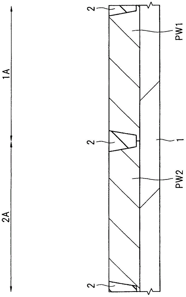
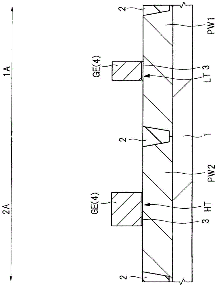
[0133] figure 1 is a main sectional view showing the configuration of the semiconductor device in this embodiment. The semiconductor device in this embodiment has MISFETs (LT) and MISFETs (HT).
[0134] The MISFET (LT) is a MISFET formed in the core MIS formation region 1A, and has a gate length smaller than that of the MISFET (HT). The gate length of the MISFET (LT) is, for example, about 40 nm when its manufacturing process belongs to the 40-nm regular stage. Such a MISFET having a relatively small gate length is used, for example, in a circuit (also referred to as a core circuit or a peripheral circuit) for driving another element such as a memory MC. The driving voltage of the MISFET (LT) tends to be smaller than that of the MISFET (HT). The insulating film 3 of the MISFET (LT) may be thinner than that o...
no. 2 example
[0199] Referring now to the drawings, a description will be given below of the structure of the semiconductor device (semiconductor memory device) in this embodiment.
[0200] -Structure Description-
[0201] Figure 20 is a main sectional view showing the configuration of the semiconductor device in this embodiment. The semiconductor device in this embodiment has a MISFET (LT) and a memory cell (also referred to as a nonvolatile memory cell, a nonvolatile memory element, a nonvolatile semiconductor memory device, an EEPROM, or a flash memory).
[0202] The MISFET (LT) is a MISFET formed in the core MIS formation region 1A, and has a relatively small gate length. For example, the gate length of the MISFET (LT) is smaller than the sum of the gate length of the control gate electrode CG of the memory cell MC and the gate length of its memory gate electrode MG, and is, for example, about 40 nm. Such a MISFET having a relatively small gate length is used, for example, in a circ...
no. 3 example
[0291] Referring now to the drawings, a description will be given below of the structure of the semiconductor device (semiconductor memory device) in this embodiment.
[0292] -Structure Description-
[0293] Figure 44 is a main sectional view showing the configuration of the semiconductor device in this embodiment. The semiconductor device in this embodiment has MISFETs (LT), MISFETs (HT), and memory cells MC.
[0294] The MISFET (LT) is a MISFET formed in the core MIS formation region 1A, and has a gate length smaller than that of the MISFET (HT). The gate length of the MISFET (LT) is, for example, about 40 nm. Such a MISFET having a relatively small gate length is used, for example, in a circuit (also referred to as a core circuit or a peripheral circuit) for driving a memory MC. The driving voltage of the MISFET (LT) tends to be smaller than that of the MISFET (HT). The insulating film 3 of the MISFET (LT) may be thinner than that of the MISFET (HT).
[0295] On the...
PUM
| Property | Measurement | Unit |
|---|---|---|
| thickness | aaaaa | aaaaa |
| thickness | aaaaa | aaaaa |
| thickness | aaaaa | aaaaa |
Abstract
Description
Claims
Application Information
 - R&D
- Intellectual Property
- Life Sciences
- Materials
- Tech Scout
- Unparalleled Data Quality
- Higher Quality Content
- 60% Fewer Hallucinations
Browse by: Latest US Patents, China's latest patents, Technical Efficacy Thesaurus, Application Domain, Technology Topic, Popular Technical Reports.
© 2025 PatSnap. All rights reserved.Legal|Privacy policy|Modern Slavery Act Transparency Statement|Sitemap|About US| Contact US: help@patsnap.com