Anti-optical aliasing semiconductor laser distance measuring device and method for traceable precise measuring ruler

A laser ranging and semiconductor technology, applied in measuring devices, radio wave measuring systems, using re-radiation, etc., can solve the problems that the laser measuring ruler cannot be directly traced to the nonlinear period, the ultra-long wavelength cannot be generated synchronously, and the error frequency. Achieve the effects of overcoming non-direct traceability, improving measurement efficiency and accuracy, and reducing frequency

Active Publication Date: 2017-07-18
HARBIN INST OF TECH
View PDF10 Cites 0 Cited by
  • Summary
  • Abstract
  • Description
  • Claims
  • Application Information

AI Technical Summary

Problems solved by technology

[0012] The purpose of the present invention is to solve the problems that the ultra-long wavelength and ultra-short wavelength cannot be synchronously generated in the existing phase laser ranging technology, the laser measuring ruler cannot be directly traced to the source, and the problems of nonlinear periodic error and frequency aliasing are provided. Anti-optical aliasing traceable precision measuring ruler semiconductor laser ranging device and method to achieve the purpose of increasing the flexibility of ranging, simplifying the steps of ranging, and improving measurement efficiency, accuracy and real-time performance

Method used


Image

  • Anti-optical aliasing semiconductor laser distance measuring device and method for traceable precise measuring ruler
  • Anti-optical aliasing semiconductor laser distance measuring device and method for traceable precise measuring ruler
  • Anti-optical aliasing semiconductor laser distance measuring device and method for traceable precise measuring ruler

Examples


Embodiment Construction

[0038] Embodiments of the present invention will be described in detail below in conjunction with the accompanying drawings.

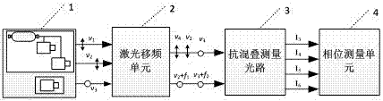
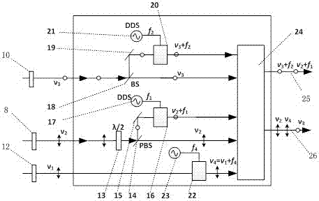
[0039] A semiconductor laser distance measuring device with anti-optical aliasing and traceable precise ruler, characterized in that the device is composed of a measuring ruler generating unit 1, a laser frequency shifting unit 2, an anti-aliasing measuring optical path 3 and a phase measuring unit 4 , where the laser output from the ruler generating unit 1 is output to the input end of the laser frequency shifting unit 2, the output reference laser beam 25 and the measuring laser beam 26 of the laser frequency shifting unit 2 are output to the anti-aliasing measurement optical path 3, and the anti-aliasing measurement Output signal I of optical path 3 3 , I 4 , I 5 , I 6 input to the phase measurement unit 4 respectively;

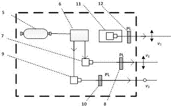
[0040] The structure of the measuring ruler generation unit 1 is: the laser beam emitted by the frequency reference laser 5 r...


PUM


Abstract

An optical aliasing prevention traceable fine measurement tape semiconductor laser ranging device and method belongs to the phase laser ranging technology. The device comprises a measuring tape generating unit, a laser frequency shift unit, an aliasing prevention measuring light path and a phase measuring unit. The method comprises the following steps of, firstly, starting a frequency reference laser device and a semiconductor laser device; secondly, taking one beam as a reference laser beam, and taking the other beam as a measuring laser beam; thirdly, taking c / Iv2-v3I as a fine measurement tape; fourthly, taking c / Iv4-v2I as a rough measurement tape; fifthly, moving a measuring pyramid prism to a target end to obtain the phase differences of (i) phi ( / i) 1 and (i) phi ( / i) 2 of the fine measurement tape and the rough measurement tape; lastly, obtaining a measured distance value through formulas. The optical aliasing prevention traceable fine measurement tape semiconductor laser ranging device and method solves the problems that superlong wavelengths and ultrashort wavelengths cannot be generated synchronously and laser tapes are incapable of performing direct tracing and have nonlinear periodic errors and frequency aliasing, and has the advantages of being high in measuring range, measuring precision, stability and practicality.

Description

technical field [0001] The invention belongs to phase laser measurement technology, and mainly relates to a phase laser distance measuring device and method. Background technique [0002] Large-scale measurement has attracted much attention in the development of large-scale precision machinery manufacturing, major scientific and technological projects, aerospace industry, shipbuilding industry and microelectronic equipment industry and other large-scale optical-mechanical-electrical integration equipment processing and manufacturing. It is an important basis for the processing and overall assembly of large parts in aerospace vehicles and giant ships. The quality of its measurement methods and equipment performance directly affect the quality of workpieces and assembly accuracy, which in turn affects the operating quality, performance and life of the entire set of equipment. The multi-ruler phase ranging method uses a group of measuring ruler wavelengths from large to small t...

Claims


Application Information

Patent Timeline
Patent Type & Authority Patents(China)
IPC IPC(8): G01S11/12
CPCG01S11/12
Inventor 谭久彬杨宏兴胡鹏程
Owner HARBIN INST OF TECH
Why Eureka
Try Eureka