Processing for electromechanical systems and equipment for same

A technology for processing chambers and equipment, used in circuits, electrical components, semiconductor/solid-state device manufacturing, etc., to solve problems such as damage sensitivity and device vulnerability

Inactive Publication Date: 2014-09-10
IDC LLC
View PDF4 Cites 7 Cited by
  • Summary
  • Abstract
  • Description
  • Claims
  • Application Information

AI Technical Summary

Problems solved by technology

After release, the device is vulnerable and suscepti

Method used


Image

  • Processing for electromechanical systems and equipment for same
  • Processing for electromechanical systems and equipment for same
  • Processing for electromechanical systems and equipment for same

Examples


Embodiment Construction

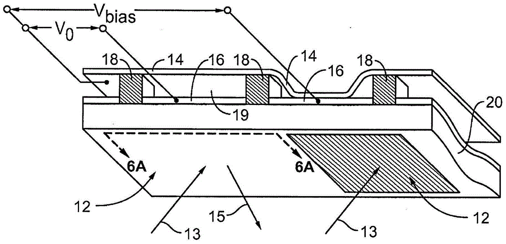
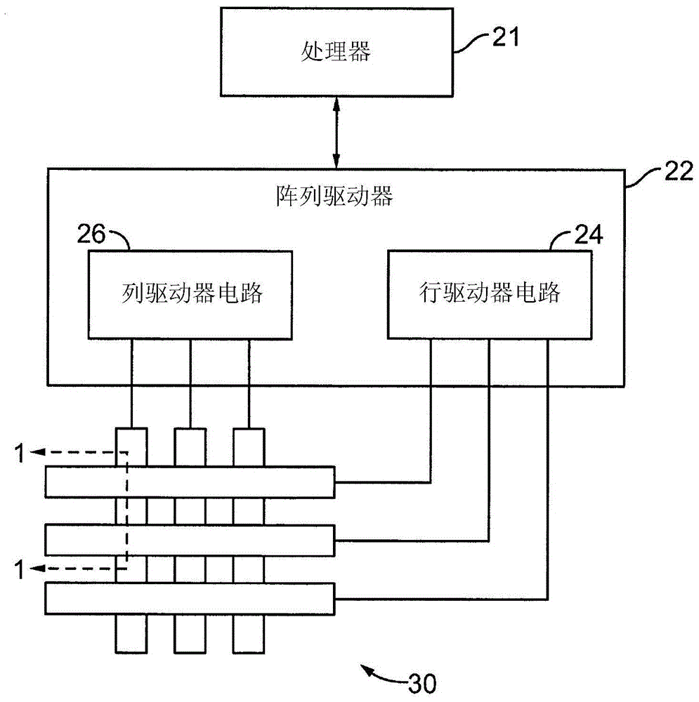
[0039] The following description is directed to certain implementations for the purpose of describing the innovative aspects of the invention. However, those skilled in the art will readily recognize that the teachings herein can be applied in a number of different ways. The described embodiments may be practiced in any device or system that can be configured to display images, whether in motion (eg, video) or stationary (eg, still images), and whether textual, graphical or pictorial. More specifically, it is contemplated that the described implementations may be included in or associated with a variety of electronic devices such as, but not limited to: mobile telephones, multimedia cellular telephones with Internet capabilities , mobile TV receivers, wireless devices, smart phones, Devices, Personal Data Assistants (PDAs), Wireless Email Receivers, Handheld or Portable Computers, Netbooks, Notebook Computers, Smartbooks, Tablet Computers, Printers, Copiers, Scanners, Fax De...


PUM


Abstract

This disclosure provides systems, methods and apparatus for processing multiple substrates in a batch cluster tool. A batch cluster tool can include a transfer chamber, an etch process chamber, and one or both of an ALD process chamber and an SAM process chamber. Each of the batch process chambers can be a common chamber where the substrates are open to one another, or can include multiple process subchambers that are isolated from one another in operation. Multiple substrates are transferred into an etch chamber. The substrates are exposed to a vapor phase etchant. The substrates can then be transferred to an atomic layer deposition (ALD) chamber and exposed to vapor phase reactants to form a thin film. The substrates can be transferred either from the etch process chamber or the ALD chamber to a third chamber and exposed to vapor phase reactants to form a self-assembled monolayer (SAM).

Description

technical field [0001] The invention relates to electromechanical systems. Background technique [0002] Electromechanical systems (EMS) include devices having each of the following: electrical and mechanical elements, actuators, transducers, sensors, optical components (eg, mirrors and optical films), and electronics. Electromechanical systems at various scales, including but not limited to microscale and nanoscale, can be fabricated. For example, microelectromechanical systems (MEMS) devices can include structures having sizes ranging from about 1 micron to hundreds of microns or more. Nanoelectromechanical systems (NEMS) can include structures having sizes smaller than 1 micron (eg, sizes smaller than hundreds of nanometers). Electromechanical elements may be created using deposition, etching, photolithography, and / or other micromachining processes that etch away portions of substrates and / or deposited material layers or add layers to form electrical and electromechanic...

Claims


Application Information

Patent Timeline
IPC IPC(8): H01L21/67
CPCH01L21/67207H01L21/67069
Inventor 笹川照夫莱昂纳德·尤金·芬内尔
Owner IDC LLC
Why Eureka
Try Eureka