

A kind of horizontal growth device and growth method of phosphorus silicon cadmium single crystal
A growth device and a technology for crystal nucleus growth, applied in the directions of single crystal growth, single crystal growth, crystal growth, etc., can solve the problems of increased cost and easy volatilization of the gold-plated layer.
- Summary
- Abstract
- Description
- Claims
- Application Information
AI Technical Summary
Problems solved by technology
Method used
Image

Examples
Embodiment 1
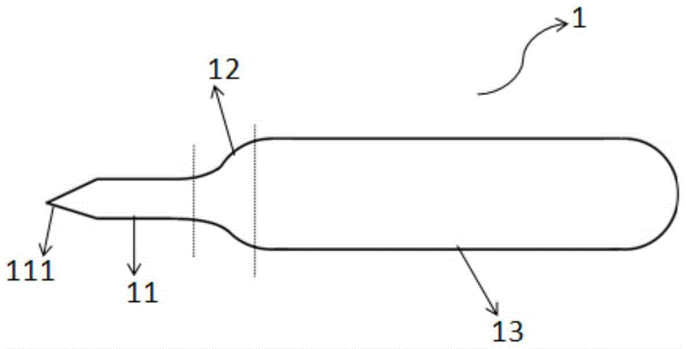
[0109] as attached figure 1 As shown, the embodiment of the present invention provides a PBN boat-shaped crucible 1 for a horizontal growth device of phosphorus, silicon, and cadmium single crystals, including: a crystal nucleus growth section 11, a transition section 12, and a single crystal growth section 13,
[0110] The first end portion of the crystal nucleus growth segment 11 is wedge-shaped with a wedge angle of 30° (see attached Figure 1a ), the second end of the crystal nucleus growth section 11, the transition section 12 and the single crystal growth section 13 are sequentially connected,
[0111] The width and length of the crystal nucleus growth section 11 are respectively 15mm and 60mm,
[0112] The width and length of the single crystal growth segment 13 are 70 mm and 200 mm, respectively.
Embodiment 2
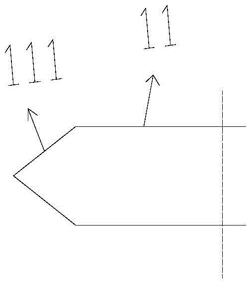
[0114] as attached figure 1 As shown, the embodiment of the present invention provides a PBN boat-shaped crucible 1 for a horizontal growth device of a phosphorus-silicon-cadmium single crystal, except that the wedge angle of the first wedge-shaped end is 70° (see attached Figure 1b ); the width and length of the crystal nucleus growth section 11 are respectively 2mm and 10mm; the width and length of the single crystal growth section 13 are respectively 5mm and 20mm. All the other structures of the crucible provided in Example 1 are the same.
Embodiment 3
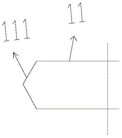
[0116] as attached figure 1 As shown, the embodiment of the present invention provides a PBN boat-shaped crucible 1 for a horizontal growth device of a phosphorus-silicon-cadmium single crystal, except that the wedge angle of the first wedge-shaped end is 150° (see the appended Figure 1c ); the width and length of the crystal nucleus growth section 11 are respectively 20mm and 80mm; the width and length of the single crystal growth section 13 are respectively 100mm and 300mm. All the other structures of the crucible provided in Example 1 are the same.
PUM
| Property | Measurement | Unit |
|---|---|---|
| microhardness | aaaaa | aaaaa |
Abstract
Description
Claims
Application Information