Memristor based on pn heterostructure and manufacturing method thereof

A technology of heterostructure and memristor, which is applied in the field of information storage, can solve the problems of limiting the initial state of the device, the control space and flexibility of the memristive properties, etc., to achieve the effect of increasing flexibility.

Active Publication Date: 2014-09-17
NORTHEAST NORMAL UNIVERSITY
View PDF4 Cites 18 Cited by
  • Summary
  • Abstract
  • Description
  • Claims
  • Application Information

AI Technical Summary

Problems solved by technology

The above two types of models often need to rely on insulating or semi-insulating materials, which may limit the choice of the initial state of the device, and the control space and flexibility of the memristive properties need to be expanded.

Method used


Image

  • Memristor based on pn heterostructure and manufacturing method thereof
  • Memristor based on pn heterostructure and manufacturing method thereof
  • Memristor based on pn heterostructure and manufacturing method thereof

Examples


Embodiment 1

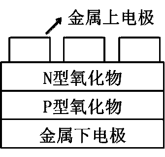
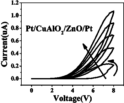
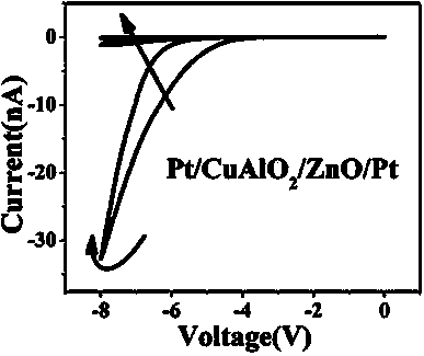
[0030] The structure and composition of Pn heterostructure memristor: as figure 1 The structure shown, in this embodiment, the upper and lower electrodes are made of inert metal Pt, and the p-type oxide is CuAlO 2 Thin films, n-type oxides are composed of ZnO thin films adhered in turn.

[0031] Preparation of the memristor: the 200nm inert metal Pt substrate is used as the bottom electrode after being cleaned by physical or chemical methods. On the lower electrode, a layer of p-type CuAlO was deposited by magnetron sputtering 2 Thin film, the thickness of the film is about 50 nanometers. The specific preparation conditions are: background vacuum: lower than 5.0×10 -4 Pa; sputtering gas: high-purity oxygen (O 2 ); growth pressure: 2Pa; sputtering target: CuAlO 2 Ceramic; sputtering power: 90W; substrate temperature: room temperature. After that, in the amorphous CuAlO 2 On the thin film, a layer of n-type ZnO thin film is also deposited by magnetron sputteri...

Embodiment 2

[0034] The structure and composition of Pn heterostructure memristor: as figure 1 As shown in the structure, in this embodiment, the lower electrode is made of inert metal Pt, the p-type oxide is NiO thin film, the n-type oxide is ZnO thin film, and the metal upper electrode Au is adhered in sequence.

[0035] Preparation of the memristor: the 200nm inert metal Pt substrate is used as the bottom electrode after being cleaned by physical or chemical methods. On the lower electrode, deposit a layer of p-type NiO thin film by magnetron sputtering method, and the film thickness is about 60 nanometers. The specific preparation conditions are: background vacuum: lower than 5.0×10 -4 Pa; sputtering gas: high-purity oxygen (O 2); growth pressure: 2Pa; sputtering target: NiO ceramics; sputtering power: 120W; substrate temperature: room temperature. Afterwards, on the NiO film, a layer of n-type ZnO film was also deposited by magnetron sputtering, with a film thickness of about 60 n...


PUM

PropertyMeasurementUnit
thicknessaaaaaaaaaa
thicknessaaaaaaaaaa
thicknessaaaaaaaaaa

Abstract

The invention belongs to the technical field of information storage, and particularly relates to a memristor based on a pn heterostructure and a manufacturing method of the memristor. The memristor comprises an upper electrode and a lower electrode, and the pn heterostructure composed of p-type oxide (such as CuAlO2 and NiO) and n-type oxide (such as ZnO and TiO2) is inserted between the upper electrode and the lower electrode. Positive bias voltages are continuously applied to the lower electrode, and oxygen ions in a depletion layer can be gradually migrated to one side of a p-type region from an n-type region. The vacancy concentration of positive ions on one side of the p-type region and the vacancy concentration of oxygen on one side of the n-type region are increased at the same time, the width of the depletion layer of a pn joint is gradually reduced, and therefore device resistance is gradually lowered, and the resistance memory behavior is achieved. The characteristic that the physical property of the pn joint is easy to modulate is utilized, and flexibility of regulating and controlling the resistance memory performance is increased. Selectivity on materials is poor, the performance of the resistance memory behavior is stable, the half-quantitative study on a resistance memory device is facilitated, and the basis is laid for device deign and further development.

Description

[0001] technical field [0002] The invention belongs to the technical field of information storage, and in particular relates to a pn heterostructure memristor and a preparation method thereof. Background technique [0003] In recent years, the biomimetic simulation of biological synaptic functions has gradually become a research hotspot. In the research of traditional neurosynaptic bionic devices, multiple transistors and capacitors are often required to simulate the function of a single synapse, which leads to the complexity of artificial neural network circuit design and high energy consumption. and would limit the number of synapses per chip to approximately 10 2 -10 5 , much lower than the 10 in the human brain 14 magnitude. This largely limits the bionic simulation of biological synapse functions. [0004] Memristors are the fourth basic passive electronic device after resistors, capacitors, and inductors. Cai Shaotang first deduced the existence of this element...

Claims


Application Information

Patent Timeline
Patent Type & Authority Applications(China)
IPC IPC(8): H01L29/8605H01L21/329
CPCH01L29/66969H01L29/8605
Inventor 徐海阳张磊王中强于浩刘益春
Owner NORTHEAST NORMAL UNIVERSITY
Why Eureka
Try Eureka