Nanosecond time-resolved absorption and emission spectrum measuring device and measuring method

An emission spectrum and time-resolved technology, which is applied in the field of instruments that measure nanosecond time-resolved absorption and emission spectra respectively, and can solve the problems of single-function spectroscopy equipment, unable to control, and only approximately equal to room temperature.

Active Publication Date: 2014-09-24
DALIAN INST OF CHEM PHYSICS CHINESE ACAD OF SCI
View PDF5 Cites 5 Cited by
  • Summary
  • Abstract
  • Description
  • Claims
  • Application Information

AI Technical Summary

Problems solved by technology

[0003] Mature commercial spectroscopic testing devices are mainly concentrated in steady-state absorption and emission spectrometers. The two most representative companies that produce this type of product are PerkinElmer of the United States (Document 3: http://www.perkinelmer.com/) and Horiba Jobin Yvon Company of France (Document 4: http://www.horiba.com/cn/), spectroscopic equipment with time-resolving function often has a single function, specifically, the existing set of equipm

Method used


Image

  • Nanosecond time-resolved absorption and emission spectrum measuring device and measuring method
  • Nanosecond time-resolved absorption and emission spectrum measuring device and measuring method
  • Nanosecond time-resolved absorption and emission spectrum measuring device and measuring method

Examples


Embodiment Construction

[0026] The present invention will be further described in detail below in conjunction with the accompanying drawings and embodiments.

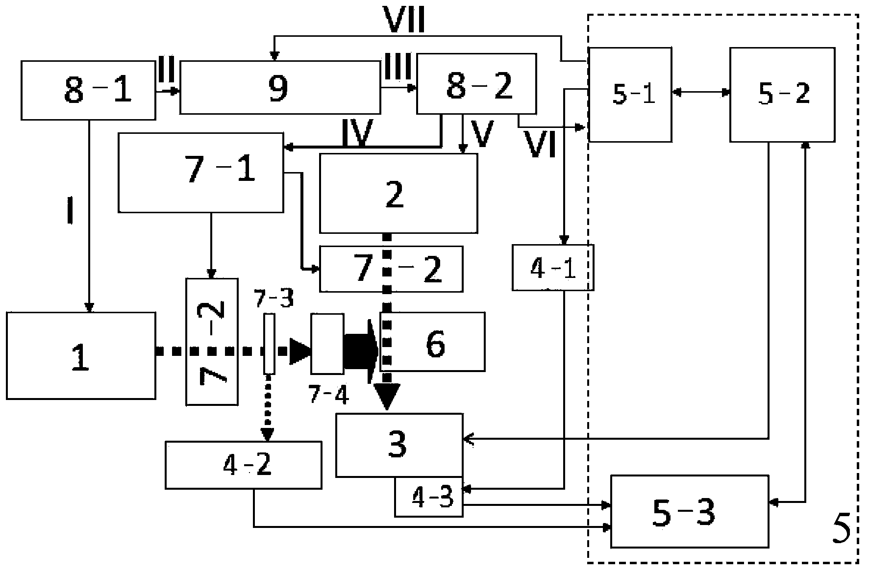
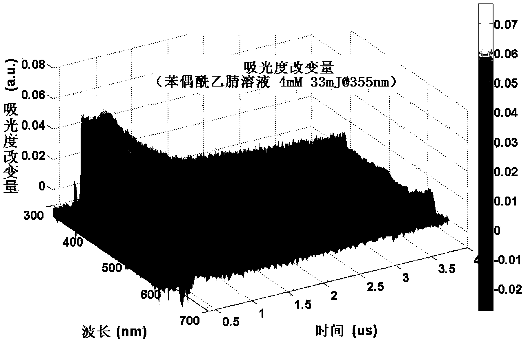
[0027] In the sample cell of the present invention, the sample is controllably set at a temperature within the range of -50°C-50°C, and the time-resolved absorption and emission spectra of the excited state of the sample are measured within the range of wavelength 200nm-900nm and time 50ns-2ms , the minimum intensity resolution is about 0.0005, and the measurement frequency is adjustable in the range of 1Hz-5Hz. In order to obtain a high signal-to-noise ratio, the present invention obtains the final experimental result by taking the average of multiple measurements, and the average times are adjustable. The device will provide reliable technical support for developing clean energy regeneration technology and exploring new solutions for environmental protection.

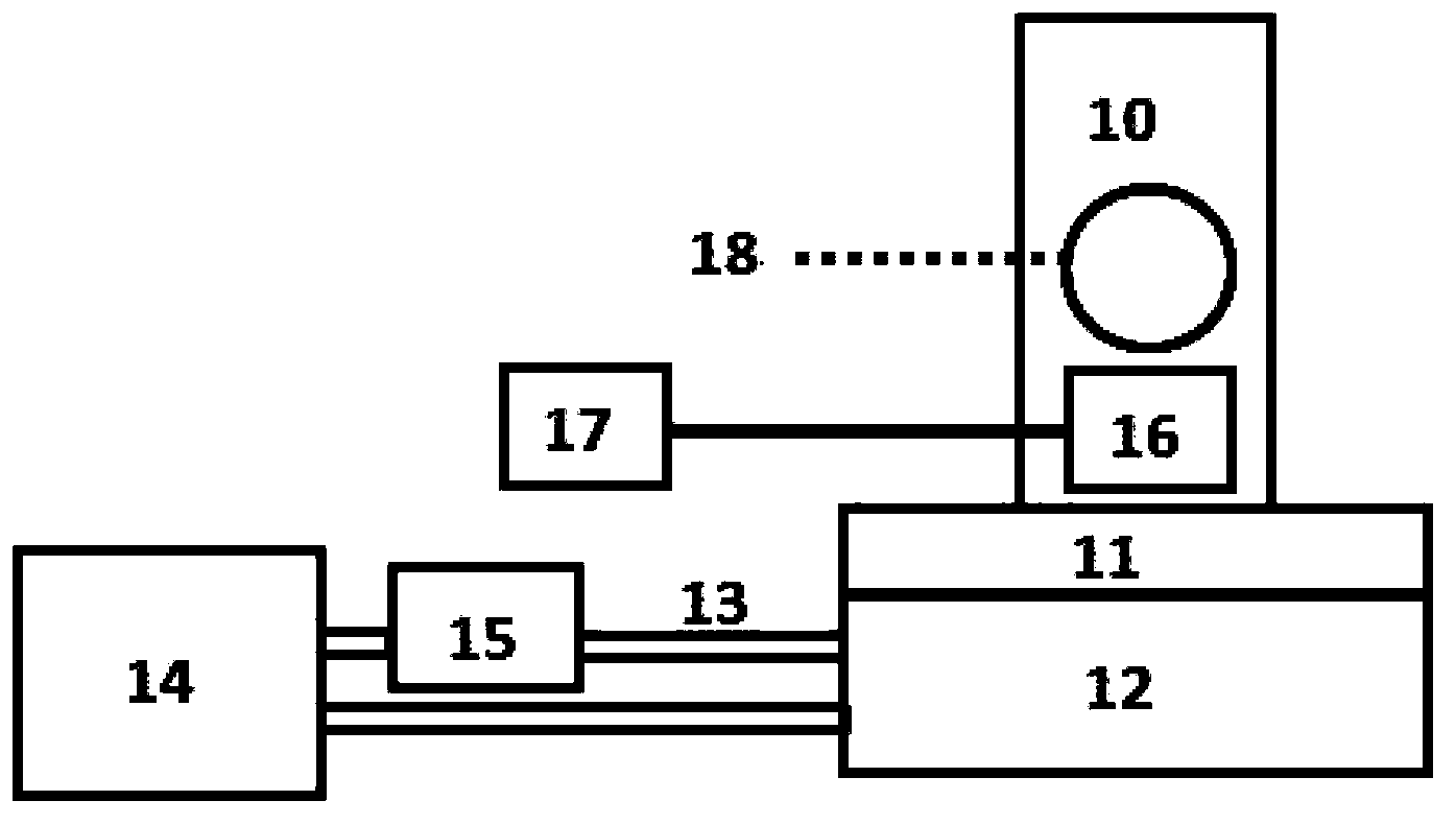
[0028] The present invention completed according to the above-mentioned purpose i...


PUM


Abstract

The invention relates to a nanosecond time-resolved absorption and emission spectrum measuring device. An excitation light source is orderly connected with a first sequence pulse generator, a working frequency coordinator, a second sequence pulse generator, and a data collector; the second sequence pulse generator is respectively connected with a light path system and a detection light source; the data collector is respectively connected with the working frequency coordinator, a first light intensity detector, a second light intensity detector, a third light intensity detector, and a monochromator; the light path system and a sample cell are also disposed between the detection light source and the monochromator. The measuring method comprises: setting the temperature of a sample, irradiating the sample by light beams emitted by the excitation light source to reach an electron excitation state, obtaining zero point time of time-resolved spectrum data by part of the light beams; after pulsed white light emitted by the detection light source passes through the sample, feeding back detection light intensity signals to the data collector, and converting the signals into absorption and emission spectra. The measuring device of the invention is equipped with a temperature controllable sample cell, and obtains spectrum data with a high signal to noise ratio.

Description

technical field [0001] The invention relates to a time-resolved spectrum measuring device and method, in particular to an instrument and method capable of measuring nanosecond time-resolved absorption and emission spectra respectively under the condition that the sample temperature can be adjusted. Background technique [0002] The photosynthesis of plants and the photodegradation of pollutants provide human beings with a source of food and a good living environment. Studying the physical and chemical processes triggered by light helps to understand these natural phenomena. New technical ideas. In general, the light-triggered chemical reaction path is: when a substance in the electronic ground state is irradiated by a light beam of a suitable wavelength, the electrons of the substance are triggered to an excited state, forming intermediates with strong reactivity, and generating electrons in different environments The final product in the ground state (Document 1: Fan Meigo...

Claims


Application Information

Patent Timeline
IPC IPC(8): G01N21/63
Inventor 徐大力韩克利刘建勇杨阳刘本康王艳秋
Owner DALIAN INST OF CHEM PHYSICS CHINESE ACAD OF SCI
Why Eureka
Try Eureka