

Preparation method for multi-state electrochromic device
A technology of electrochromic devices and conductive layers, which is applied in the fields of instruments, optics, nonlinear optics, etc., and can solve the problems of unfavorable practical application in industrial fields, high cost of nano-indium tin oxide, etc.
- Summary
- Abstract
- Description
- Claims
- Application Information
AI Technical Summary
Problems solved by technology
Method used
Image

Examples
Embodiment 1
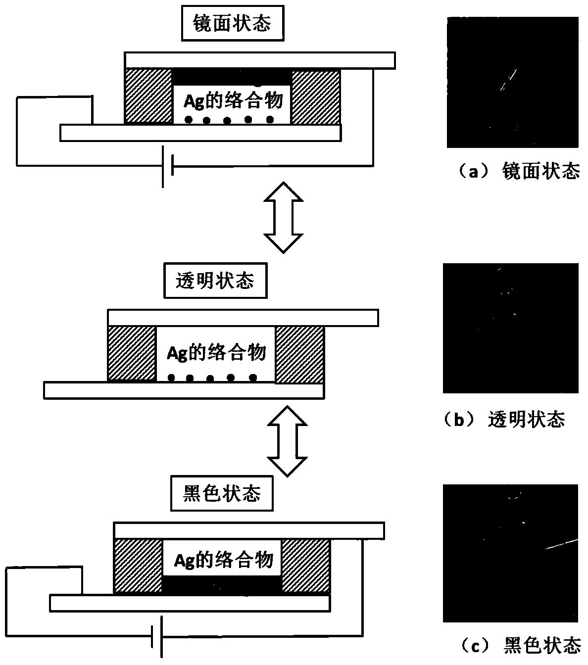
[0023] Step 1: Weigh 85mg (0.5mmol) of AgNO 3 , 806mg (2.5mmol) of tetrabutylammonium bromide (TBABr), 13mg (0.1mmol) of CuCl 2 , it was dissolved in 10mL of DMSO, and magnetically stirred until the solute was completely dissolved;
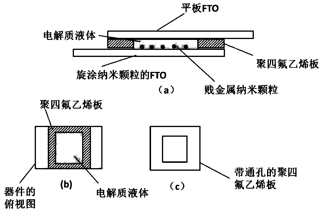
[0024] Step 2: Select two pieces of FTO glass with a size of 3cm×2.5cm as electrodes, soak them in deionized water and ethanol in turn, and clean them 5 times with an ultrasonic cleaner, and then dry them at 80°C ,spare;
[0025] Step 3: Take a PTFE plate with a size of 2.5cm×2.5cm and a thickness of 5mm, dig a 2cm×2cm through hole in the middle, and then rinse the PTFE with deionized water and absolute ethanol respectively plate 4 times, and then dried at 60°C for later use;
[0026] Step 4: Weigh 0.5g of TiO 2 Nanoparticles, the particle size is 20nm, dissolved in 10mL of absolute ethanol (purity ≥ 99.7%), ultrasonic vibration for 30min, until TiO 2 Evenly dispersed in the solution. Take any piece of FTO glass in step 2, cover the short si...
Embodiment 2
[0030] Step 1: Weigh 127.5mg (1mmol) of AgNO 3 , 1612mg (5mmol) of tetrabutylammonium bromide (TBABr), 26mg (0.2mmol) of CuCl 2 , it was dissolved in 20mL of DMSO, and magnetically stirred until the solution was completely dissolved;
[0031] Step 2: Select two pieces of FTO glass with a size of 5.5cm×5cm as electrodes, soak them in deionized water and ethanol in turn, and clean them 5 times with an ultrasonic cleaner. After cleaning, dry at 80°C and set aside;
[0032] Step 3: Take a PTFE plate with a size of 5cm×5cm and a thickness of 5mm, dig a 4.5cm×4.5cm through hole in the middle, and then rinse the PTFE with deionized water and absolute ethanol respectively plate 4 times, and then dried at 60°C for later use;
[0033] Step 4: Weigh 1g of TiO 2 Nanoparticles, the particle size is 150nm, dissolved in 20mL of absolute ethanol (purity ≥ 99.7%), ultrasonic vibration for 30min, until TiO 2 Evenly disperse in the solution, take any piece of FTO glass in step 2, cover a la...
Embodiment 3
[0037] Step 1: Weigh 255mg (2mmol) of AgNO 3 , 3224mg (10mmol) of tetrabutylammonium bromide (TBABr), 52mg (0.4mmol) of CuCl 2 , was dissolved in 40 mL of DMSO, and magnetically stirred until the solute was completely dissolved.
[0038] Step 2: Select two pieces of FTO glass with a size of 10.5cm×10cm as electrodes, soak them in deionized water and ethanol in turn, clean them with an ultrasonic cleaner for 5 times, and dry them at 80°C after cleaning ,spare;
[0039] Step 3: Take a PTFE plate with a size of 10cm×10cm and a thickness of 5mm, dig a 9.5cm×9.5cm through hole in the middle, and then rinse the PTFE with deionized water and absolute ethanol respectively plate 4 times and then dried at 60°C for later use;
[0040] Step 4: Weigh 1g of TiO 2 Nanoparticles, the particle size is 50nm, dissolved in 20mL of absolute ethanol (purity ≥ 99.7%), ultrasonic vibration for 30min, until TiO 2 Evenly disperse in the solution, take any piece of FTO glass in step 2, cover a laye...
PUM
| Property | Measurement | Unit |
|---|---|---|
| thickness | aaaaa | aaaaa |
Abstract
Description
Claims
Application Information