Multi-chip package structure

A packaging structure, multi-chip technology, applied in the direction of electrical components, electrical solid devices, circuits, etc., can solve the problems of difficulty in pulling out electroplating wires, easy crosstalk of signals, increased processing costs, etc., to achieve easy internal routing design, reduce The difficulty of packaging process and the effect of ensuring signal integrity

Inactive Publication Date: 2014-10-01
GERAD TECH SUZHOU
View PDF4 Cites 2 Cited by
  • Summary
  • Abstract
  • Description
  • Claims
  • Application Information

AI Technical Summary

Problems solved by technology

However, due to the external limitation of the thickness of the entire package, the thickness of the chip needs to be thinned, which increases the risk of chip chipping and increases the cost of the packaging factory.
In addition, because the FBGA package uses wire bonding on one side of the package substrate, and the number of stacked layers is large, the span of the wire arc is relatively large, resulting in a relatively large amount of gold wire, and in the plastic packaging, it is easy to short circuit between the wire arcs, further increased processing costs
In addition, when there are many signal networks in the system, the wiring between each network is relatively dense. Due to the structural limitations of the traditional FBGA package, it is often necessary to design more than four layers of package substrates, and its cost will greatly increase; and because The signal is too dense, and crosstalk between signals is prone to occur, which affects the integrity of the signal, especially for DRAM high-speed signals
There is also the traditional wire bonding process. In order to improve the manufacturing capacity of the product, the package substrate needs to be electroplated. There must be electroplating wires on the substrate to conduct current for electroplating; however, due to structural limitations, the traditional FBGA package cannot be pulled out. Plating wires is difficult, so it is often necessary to use NPL (Non Plating Line, non-plated wires) process, resulting in a further increase in packaging costs

Method used


Image

  • Multi-chip package structure
  • Multi-chip package structure
  • Multi-chip package structure

Examples


Embodiment Construction

[0025] The present invention will be described in detail below in conjunction with various embodiments shown in the drawings. However, these embodiments do not limit the present invention, and any structural, method, or functional changes made by those skilled in the art according to these embodiments are included in the protection scope of the present invention.

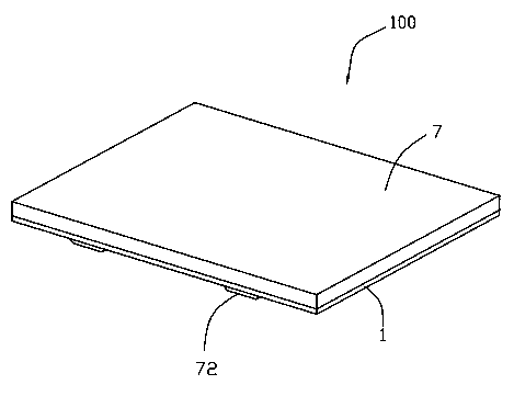
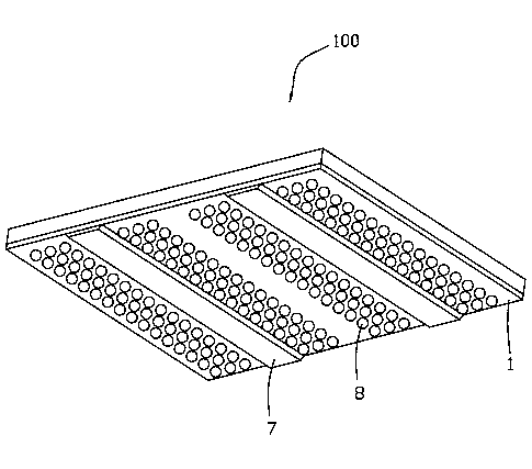
[0026] Please refer to Figure 2 to Figure 7 Shown is a preferred embodiment of the multi-chip package structure 100 of the present invention.

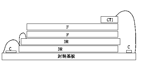
[0027] The multi-chip package structure 100 includes a substrate 1, two DRAM chips 2, a second chip 3, a circuit adapter board 4, a third chip 5, several capacitors and resistors 6, several bonding wires, a package body 7 and several tin Ball 8.

[0028] Please refer to Figure 6 and Figure 7 As shown, the substrate 1 is provided with a first surface 11 and a second surface 12 opposite to each other, a number of wires (not shown) arranged on the first surface 11 and th...


PUM


Abstract

The invention provides a multi-chip package structure which comprises a substrate, at least two DRAM chips, a first bonding wire, a second chip, a second bonding wire and a package body. The substrate is provided with a first surface, a second surface, a plurality of wires and at least two windows, wherein the first surface and the second surface are opposite, the wires are arranged on the first surface and the second surface, and the windows penetrate through the first surface and the second surface. The at least two DRAM chips are arranged on the first surface of the substrate and cover one ends of the windows respectively. The first bonding wire penetrates through the windows and is electrically connected with the DRMA chips and the wires on the second surface of the substrate. The second chip is stacked on the DRMA chips, the second bonding wire is electrically connected to the second chip and the wires on the first surface of the substrate, and the package body is packaged on the periphery of the DRAM chips and the second chip and the periphery of the windows of the substrate and covers the first bonding wire and the second bonding wire.

Description

technical field [0001] The invention relates to the technical field of semiconductor packaging, in particular to a multi-chip packaging structure. Background technique [0002] The packaging technology of DRAM has undergone several changes, from Dual Inline-pin Package (DIP), Small Outline J-Leaded Package (Small Out-Line J-Leaded Package; SOJ), thin and small High-performance packages such as Thin Small Outline Package (TSOP), Bottom Leaded Plastic (BLP), Ball Grid Array (BGA) and System in Package (SiP) era. Among them, system-in-package is a method of mechanically and electrically packaging more than two chips, packaged devices or circuits; it can double the memory capacity or realize electronic design functions in a limited space, solving space, interconnection The limited problem is the mainstream of current semiconductor packaging. Under the condition of cost permitting, the use of system-in-package technology can increase the capacity of DRAM, or expand the memory ...

Claims


Application Information

Patent Timeline
Patent Type & Authority Applications(China)
IPC IPC(8): H01L23/49
CPCH01L2224/48145H01L2224/48091
Inventor 徐健侯建飞韩邵堂
Owner GERAD TECH SUZHOU
Why Eureka
Try Eureka