Pixel array of CMOS image sensor

An image sensor and pixel array technology, applied in the field of pixel arrays, can solve problems such as poor response, and achieve the effects of less noise, excellent color digital images, and crosstalk suppression

Inactive Publication Date: 2014-10-08
SHANGHAI INTEGRATED CIRCUIT RES & DEV CENT +1
View PDF3 Cites 6 Cited by
  • Summary
  • Abstract
  • Description
  • Claims
  • Application Information

AI Technical Summary

Problems solved by technology

However, BSI still cannot completely solve the problem of poor response when light is incident obliquely

Method used


Image

  • Pixel array of CMOS image sensor
  • Pixel array of CMOS image sensor
  • Pixel array of CMOS image sensor

Examples


Embodiment Construction

[0029] The specific embodiment of the present invention will be further described in detail below in conjunction with the accompanying drawings.

[0030] It should be noted that, in the following examples, when describing the implementation of the present invention in detail, in order to clearly show the structure of the present invention for the convenience of description, the structures in the figures are not drawn according to the general scale, and partial Magnification and deformation processing, therefore, should be avoided as a limitation of the present invention.

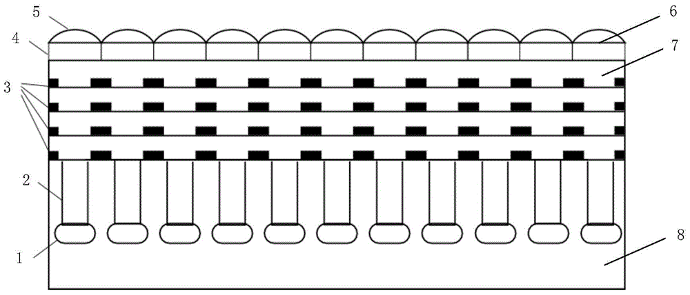
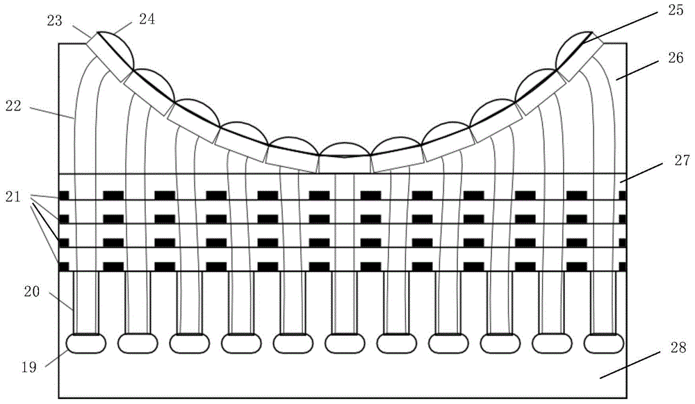
[0031] In this example, see image 3 , image 3 It is a structural schematic diagram of a pixel array of a CMOS image sensor in the present invention. like image 3 As shown, the pixel array of the present invention is an FSI pixel array, which sequentially includes a photosensitive layer 28 , a metal layer 27 , a support layer 26 and a filter layer 25 in the direction facing the lens of the camera imagin...


PUM


Abstract

The invention discloses a pixel array of a CMOS image sensor. A filter layer is in a concave hook face shape facing a camera lens and is supported by a supporting layer, a photosensitive coating and a metal layer are in a plane shape, an increased incident angle can be obtained when inclined light rays emitted into through the camera lens enter the filter layer on the edge portion close to the filter layer, the inclined light rays are conducted into a photosensitive diode through an optical fiber, obvious light intensity loss of the incident light in an optical channel can be avoided, incident optical signals can be efficiently transmitted, the imaging quality is greatly improved, the crosstalk of pixels can be effectively restrained, simpler lens design can be further matched for an optical structure, the flange focus of a main lens can be shortened, and the size of the whole imaging system can be reduced.

Description

technical field [0001] The present invention relates to a CMOS image sensor, and more particularly, to a pixel array of the CMOS image sensor. Background technique [0002] Image sensors are devices that convert light signals into electrical signals, and are widely used in digital TV and visual communication markets. According to different photoelectric conversion methods, image sensors can generally be classified into two types: charge-coupled device image sensor (Charge-coupled Device, CCD) and CMOS image sensor (CMOS IMAGE SENSOR, CIS). [0003] For CCDs, on the one hand, in professional scientific research and industrial fields, CCDs with high signal-to-noise ratio are the first choice; on the other hand, in the field of high-end photography, CCDs that can provide high image quality are also popular. For CIS, it has also been widely used in network cameras and mobile phone camera modules. [0004] Compared with CIS, CCD has higher power consumption and greater difficul...

Claims


Application Information

Patent Timeline
Patent Type & Authority Applications(China)
IPC IPC(8): H01L27/146
Inventor 陈嘉胤
Owner SHANGHAI INTEGRATED CIRCUIT RES & DEV CENT
Why Eureka
Try Eureka