

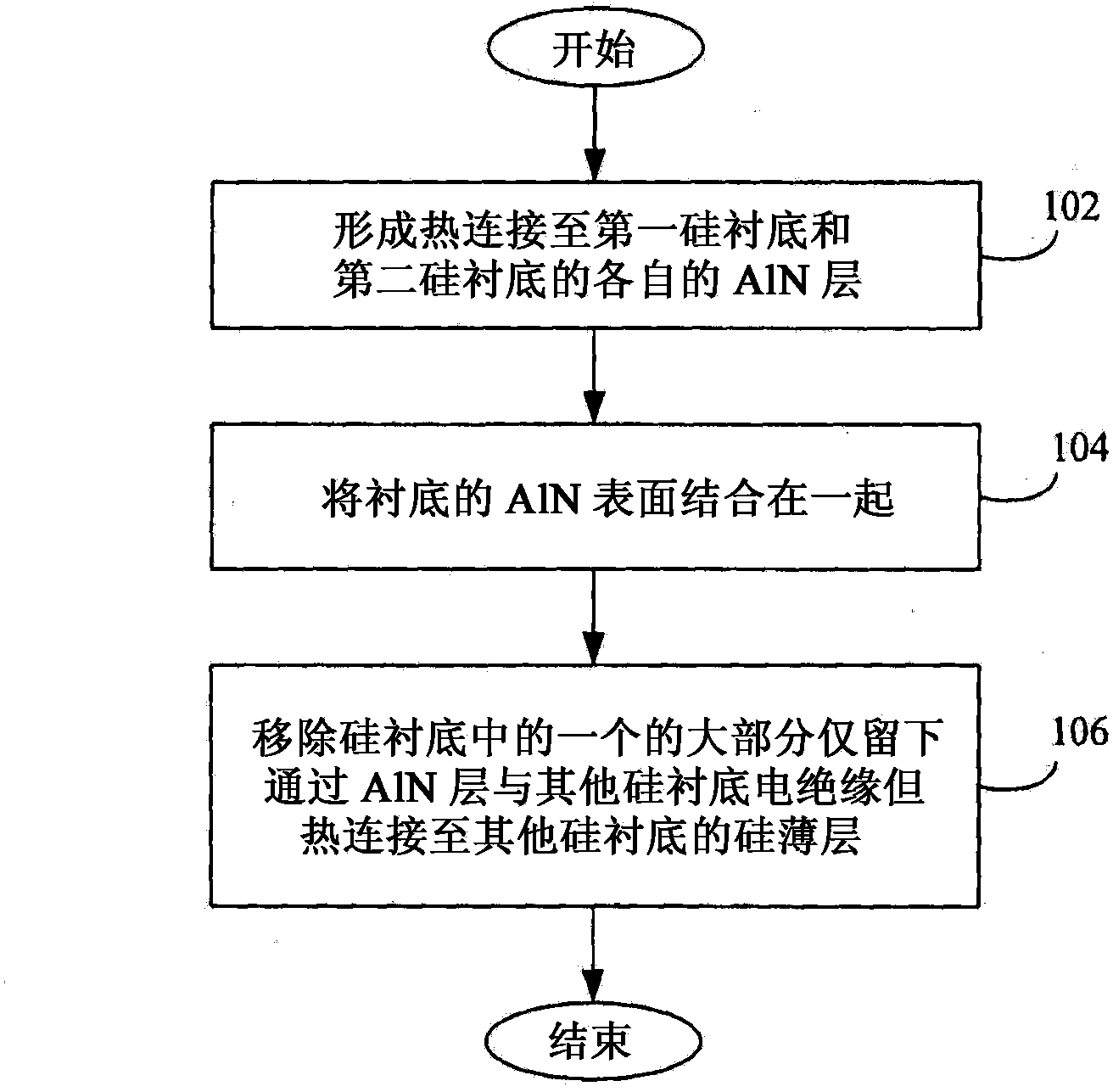
Method of producing silicon-on-insulator article
A technology of silicon-on-insulator and products, applied in the field of manufacturing of silicon-on-insulator products or products, SOI products or products, can solve problems such as poor thermal conductivity and shorten the service life of devices
- Summary
- Abstract
- Description
- Claims
- Application Information
AI Technical Summary
Problems solved by technology
Method used
Image

Examples
Embodiment
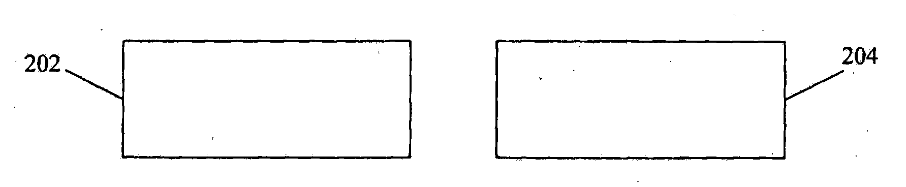
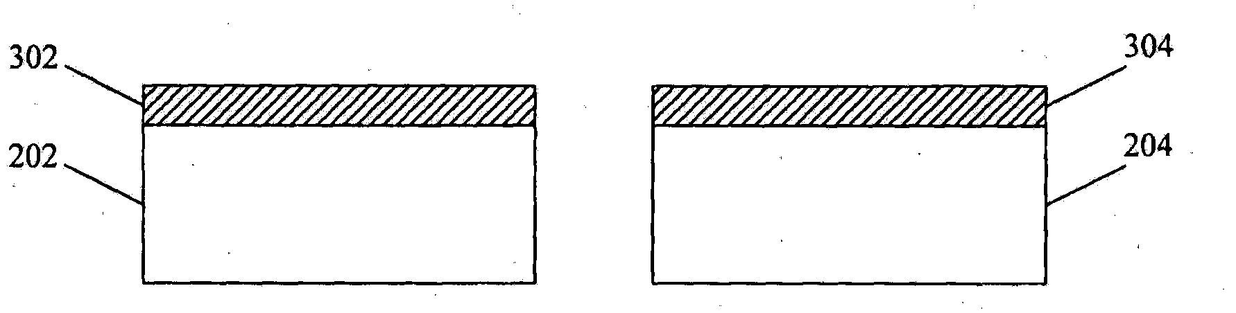
[0067] A 200 nm thick AlN layer 702, 704 was deposited simultaneously on the clean silicon surfaces of the two silicon wafers 706, 708 by reactive sputtering (RS) at a temperature of about 300°C. Wafers 706, 708 are 600 [mu]m thick, bulk single crystal wafers with 100 Ohm-cm. Both wafers 706, 708 have a (100) crystallographic orientation. Both AlN layers 702, 704 are grown with nitrogen-rich surfaces to reduce oxidation, thereby increasing the bonding strength between the two AlN layers 702, 704.
[0068] Such as Figure 7 As shown, (only) a silicon wafer 708 is then ion implanted using hydrogen ions 710 through the AlN layer 704 to 6×10 at 150 keV 16 cm -2 energy density or magnetic recording density. This forms a buried hydrogen layer 712 at a depth 714 of about 1.21±0.01 μm below the wafer surface, ie, about 1.0 μm below the AlN:Si interface.
[0069] Such as Figure 8 As shown, AlN layers 702, 704 were then face-to-face bonded using a Karl Suss SB6VAC wafer bonder at...
PUM
 Abstract
Description
Claims
Application Information