Mems Pressure Sensor, Electronic Device, Altimeter, Electronic Apparatus, And Moving Object

A technology for pressure sensors and electronic equipment, applied in piezoelectric/electrostrictive/magnetostrictive devices, electrical components, piezoelectric effect/electrostrictive or magnetostrictive motors, etc. and other problems to achieve the effect of reliable detection

Inactive Publication Date: 2014-10-22
SEIKO EPSON CORP
View PDF1 Cites 12 Cited by
  • Summary
  • Abstract
  • Description
  • Claims
  • Application Information

AI Technical Summary

Problems solved by technology

[0004] However, in the pressure sensor with the strain sensitive element disclosed in Patent Document 1, the silicon wafer needs to be thinned, and it is difficult to achieve an interface with the semiconductor device (IC) that is the calculation unit that processes the signal from the pressure sensor. integration

Method used


Image

  • Mems Pressure Sensor, Electronic Device, Altimeter, Electronic Apparatus, And Moving Object
  • Mems Pressure Sensor, Electronic Device, Altimeter, Electronic Apparatus, And Moving Object
  • Mems Pressure Sensor, Electronic Device, Altimeter, Electronic Apparatus, And Moving Object

Examples


no. 1 Embodiment approach )

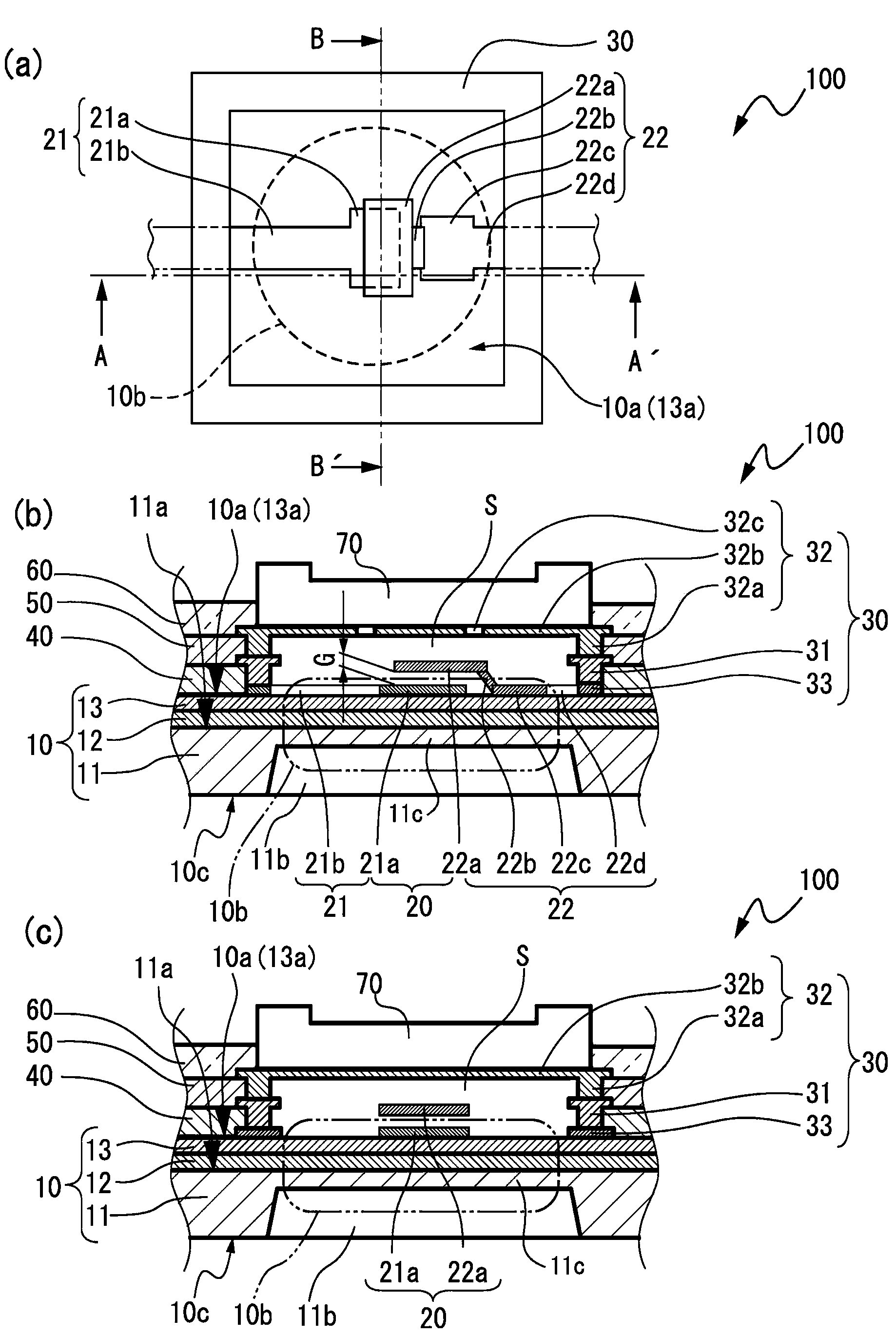
[0039] figure 1 The MEMS pressure sensor of the first embodiment is shown, (a) is a plan view in a state where a cover layer described later is penetrated, (b) is a cross-sectional view of the AA' portion shown in (a), and (c) is ( a) Cross-sectional view of part BB' shown. like figure 1 As shown in (b), the MEMS pressure sensor 100 of this embodiment has a substrate 10 consisting of a wafer substrate 11, a first oxide film 12 formed on the main surface 11a of the wafer substrate 11, and a first oxide film formed on the first oxide film. The nitride film 13 on the 12 constitutes. The wafer substrate 11 is a silicon substrate, and is also used as the wafer substrate 11 for forming a so-called IC, which is a semiconductor device described later.

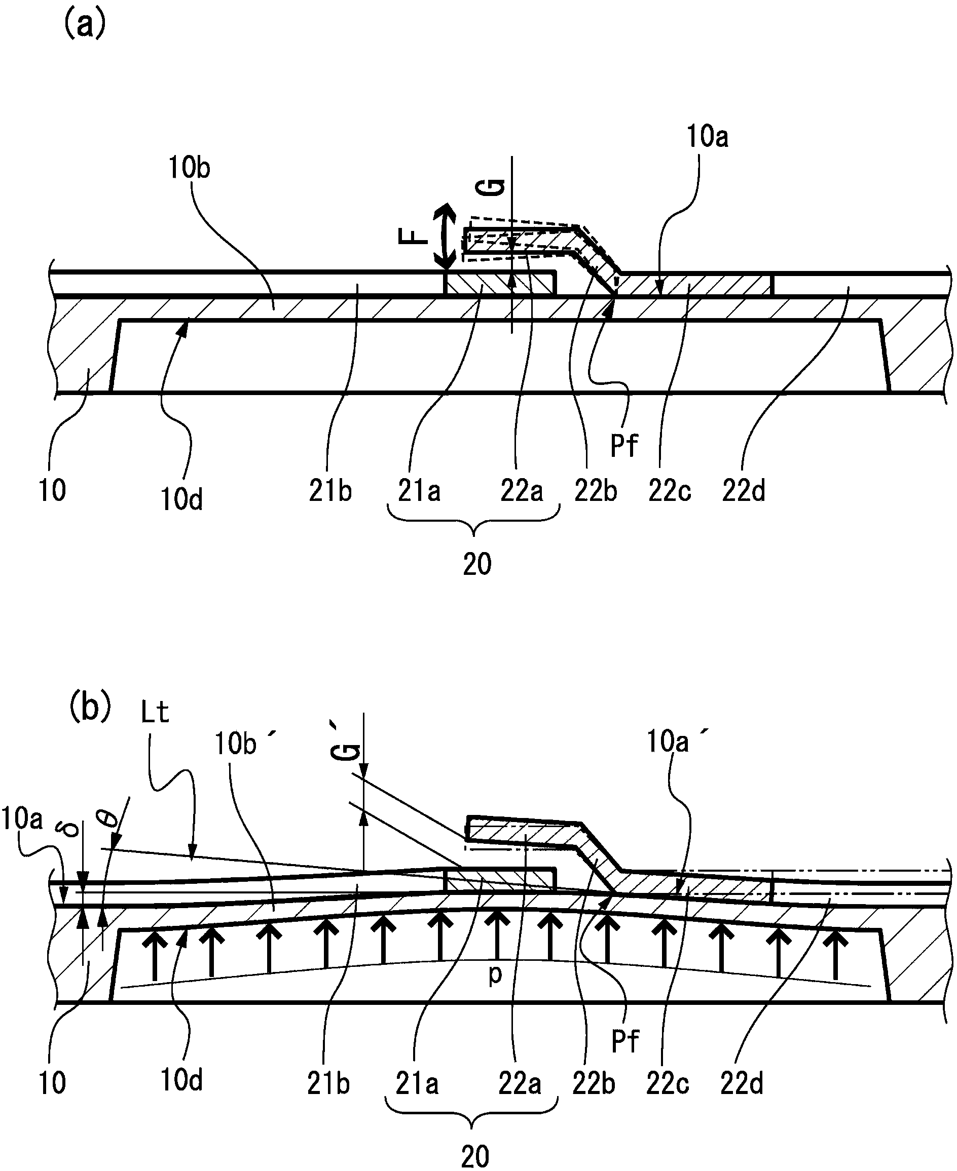
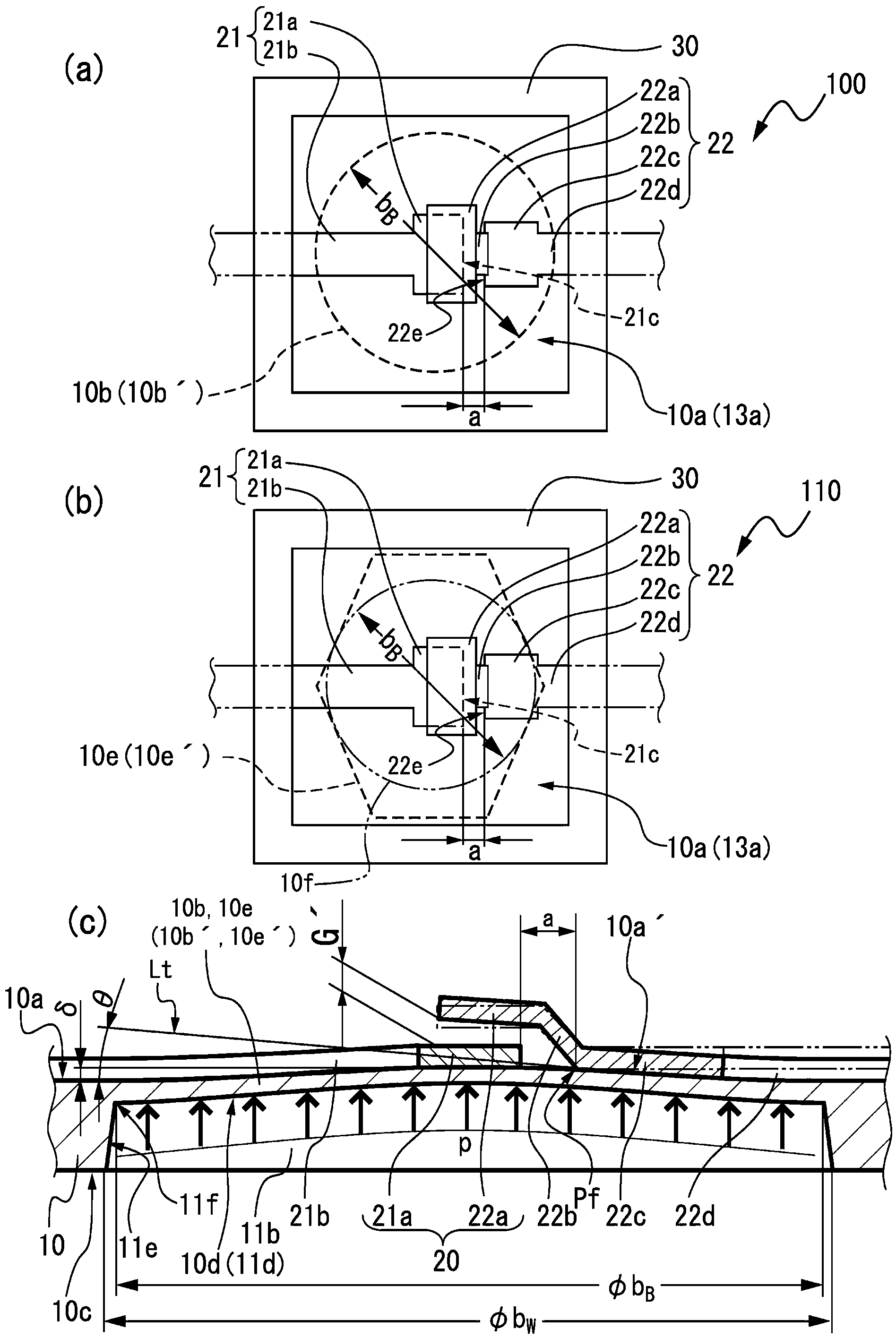
[0040] The MEMS vibrator 20 as a resonator is formed on the main surface 10 a which is the first surface of the substrate 10 , that is, the front surface 13 a of the nitride film 13 . MEMS vibrator 20 consists of figure 1The first...

no. 2 Embodiment approach )

[0073] An altimeter will be described based on the drawings as a second embodiment. The altimeter of the second embodiment is one form of electronic equipment having a pressure sensor as an electronic device including the MEMS pressure sensors 100 , 110 , 200 , and 300 of the first embodiment.

[0074] like Figure 7 As shown in (a), the altimeter 1000 according to the second embodiment has, in the case 1100 , the MEMS pressure sensor 300 according to the first embodiment; 1200; and a calculation unit 1300 as a data processing unit for calculating the data signal obtained from the MEMS pressure sensor 300 into height data. The diaphragm portion 10b of the MEMS pressure sensor 100 provided in the MEMS pressure sensor 300 is provided in the housing 1100 (refer to figure 1 ) an opening 1100a capable of communicating with the atmosphere.

[0075] Figure 7 (b) shows Figure 7 The details of the section D shown in (a), that is, the mounting section of the MEMS pressure sensor ...

no. 3 Embodiment approach )

[0081] A navigation system as an electronic device having the MEMS pressure sensor 100 , 110 , 200 , 300 of the first embodiment or the altimeter 1000 of the second embodiment, and an automobile as one embodiment of a mobile body equipped with the navigation system will be described.

[0082] Figure 9It is an external view of a mobile vehicle 4000 having a navigation system 3000 as an electronic device. The navigation system 3000 includes: map information not shown; a location information acquisition unit from a GPS (Global Positioning System: Global Positioning System); an autonomous navigation unit based on a gyro sensor, an acceleration sensor, and vehicle speed data; and the second embodiment. The altimeter 1000 and the navigation system 3000 display predetermined position information or route information on a display unit 3100 arranged at a position visually observed by the driver.

[0083] exist Figure 9 In the car 4000 shown, the navigation system 3000 has the altim...


PUM


Abstract

A MEMS pressure sensor includes a diaphragm portion that becomes displaced according to a pressure, and a resonator arranged on a main surface of the diaphragm portion. The resonator includes: a first fixed electrode provided on the main surface; and a drive electrode having a second fixed electrode provided on the main surface, a movable electrode spaced apart from the first fixed electrode, overlapping with the first fixed electrode, as viewed in a plan view seen from a normal direction to the main surface, and driven in a direction that intersects the main surface, and a supporting electrode supporting the movable electrode and connected to the second fixed electrode.

Description

technical field [0001] The present invention relates to a MEMS pressure sensor, an electronic device, an altimeter, an electronic device and a moving body. Background technique [0002] Conventionally, a semiconductor pressure sensor disclosed in Patent Document 1 is known as a device for detecting pressure. In the semiconductor pressure sensor disclosed in Patent Document 1, a strain sensitive element is formed on a silicon wafer, and the diaphragm is formed by grinding the surface of the silicon wafer opposite to the surface on which the strain sensitive element is formed to make it thinner. The strain generated in the diaphragm part displaced by the pressure is converted into a pressure. [0003] [Patent Document 1] Japanese Patent Laid-Open No. 2001-332746 [0004] However, in the pressure sensor with the strain sensitive element disclosed in Patent Document 1, the silicon wafer needs to be thinned, and it is difficult to achieve an interface with the semiconductor dev...

Claims


Application Information

Patent Timeline
Patent Type & Authority Applications(China)
IPC IPC(8): B81B7/02H03H9/205G01L1/10G01C5/06
CPCG01L9/0016G01L9/008
Inventor 北野洋司
Owner SEIKO EPSON CORP
Why Eureka
Try Eureka