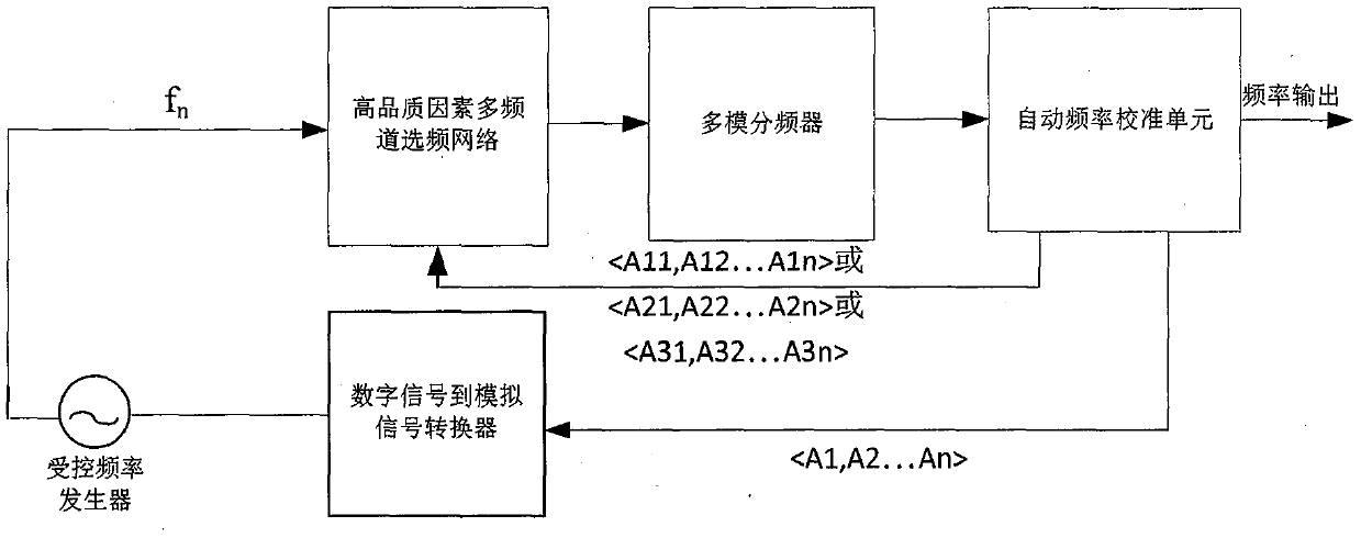
Device for realizing multi-mode clock reference source
A clock reference and multi-mode frequency divider technology, applied in the direction of electrical components, automatic power control, etc., can solve the problems that the clock reference source cannot be integrated in the chip system, increase equipment costs, etc., and achieve power consumption, area, and device cost savings Effect of low, high clock accuracy
- Summary
- Abstract
- Description
- Claims
- Application Information
AI Technical Summary
Problems solved by technology
Method used
Image

Examples
Embodiment 1
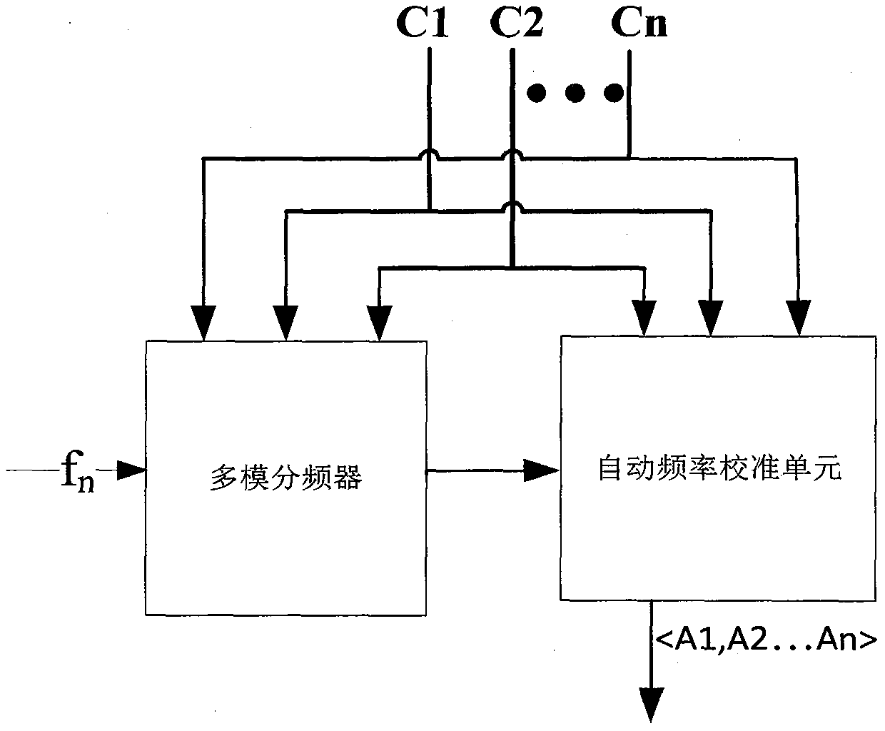
[0025] Figure 7 It is a realization block diagram of the multimode frequency divider of embodiment 1. The multi-mode frequency divider in this device is composed of three multi-mode frequency dividers, and there are 8 control bits respectively s3, s2, s1, c3, c2, c1, d2, d1. Among them, different logical combinations of the multi-mode frequency divider 1, the multi-mode frequency divider 2 and the multi-mode frequency divider 3 can realize N1, N2 and N3 frequency divisions respectively. The input frequency is f n , after frequency division, the final output frequency is f n / N (where N=N1*N2*N3). Figure 6 It is the circuit diagram of the multimode frequency divider of embodiment 1, and this frequency divider is by 4 D flip-flops (D1, D2, D3, D4), 3 inverters (1, 2, 3), 4 NOR Gates (21, 22, 23, 24), three NAND gates (31, 32, 33), and an XOR gate (41). After cascading three multi-mode frequency dividers, the frequency division coefficients that can be realized are 40, 48,...
Embodiment 2
[0029] Figure 9 It is the realization block diagram of the multimode frequency divider of embodiment 2. The multi-mode frequency divider in this device is composed of two multi-mode frequency dividers and a single-mode frequency divider, and has 6 control bits, namely s3, s2, s1, c3, c2, c1. The single-mode frequency divider is composed of two D flip-flops, which can realize frequency division by 4. The structure of the two multi-mode frequency dividers is the same as that of the multi-mode frequency divider in Embodiment 1.
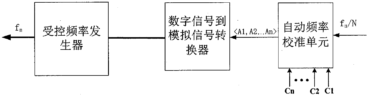
[0030] Figure 10 It is a partial circuit diagram of the automatic frequency calibration unit in Embodiment 2. The control bits s3, s2, s1, c3, c2, and c1 are simultaneously used as digital input signals of the automatic frequency calibration unit, and two digital signals A2, A1 are output through the logic circuit, and the implementation of the output terminal A1 is the input signal of the inverter 15 The output signal of the NAND inverter 16 is use...
PUM
 Abstract
Description
Claims
Application Information
 - R&D
- Intellectual Property
- Life Sciences
- Materials
- Tech Scout
- Unparalleled Data Quality
- Higher Quality Content
- 60% Fewer Hallucinations
Browse by: Latest US Patents, China's latest patents, Technical Efficacy Thesaurus, Application Domain, Technology Topic, Popular Technical Reports.
© 2025 PatSnap. All rights reserved.Legal|Privacy policy|Modern Slavery Act Transparency Statement|Sitemap|About US| Contact US: help@patsnap.com