Method for manufacturing printed circuit board by using novel and improved semi-additive process

A printed circuit board, semi-additive technology, applied in the direction of multi-layer circuit manufacturing and the formation of electrical connection of printed components, can solve the problems of reduced reliability of circuit boards, reduced thickness of electroplated copper layers, and high cost. The effect of flash erosion and thickness reduction

Inactive Publication Date: 2014-10-22
SHANGHAI MEADVILLE SCI & TECH
View PDF1 Cites 30 Cited by
  • Summary
  • Abstract
  • Description
  • Claims
  • Application Information

AI Technical Summary

Problems solved by technology

For the subtractive process, the biggest disadvantage is that during the etching process, the exposed copper layer is also etched to the side during the downward etching process (ie, side etching). applications are limited
The disadvantage of this method is that special materials such as ABF must be used, and this special material is much more expensive than traditional FR-4, RCC, etc., so the production cost is very high
The customer has clear regulations on the copper thickness of the circuit. Therefore, in order to meet the customer's requirements, it is necessary to increase the plating time and increase the thickness of the circuit during graphic electroplating, which increases the cost.
[0017] (3) In addition, during the flash corrosion process, the flash corrosion potion also has an etching effect on the orifice of the through hole and the copper on the hole wall, and because the flow rate of the flash corrosion potion at the through hole is large, the potion exchange is relatively fast, resulting in the through hole orifice The copper at the place and the hole wall is thinned, the copper thickness is significantly reduced, and the reliability of the circuit board is reduced
In actual production, try to use a method to solve this problem, that is: paste the anti-corrosion film on the position of the through hole before the flash etching to prevent the flash etching potion from etching the copper on the hole and the hole wall, but this method exists Two problems: first: the alignment problem is involved when attaching the resist film, and it is difficult to align the exposure position of the resist film with the position of the through hole; second: after the resist film is pasted on the through hole, due to the inside and The pressure outside the hole is inconsistent, and the film is easily damaged. Once the film is damaged, the electroplating layer at the corner of the through hole wall will not be protected, and the thickness of the electroplated copper layer on the hole wall and the through hole will be reduced.

Method used


Image

  • Method for manufacturing printed circuit board by using novel and improved semi-additive process
  • Method for manufacturing printed circuit board by using novel and improved semi-additive process
  • Method for manufacturing printed circuit board by using novel and improved semi-additive process

Examples


Embodiment 1

[0065] see Figure 16 ~ Figure 25 , the present invention is based on an improved semi-additive method, and the copper foil with low roughness (Rz less than 4 μm) of the laminated rough surface (copper foil has a smooth surface and a rough surface, wherein the rough surface is laminated with a dielectric layer) is thinned to 0.2-5μm, forming a thinned copper foil with Rz less than 4μm, and after pattern electroplating, use a metal protection layer to protect the circuit pattern and through holes, and remove the protection layer after flash etching.

[0066] The specific steps are:

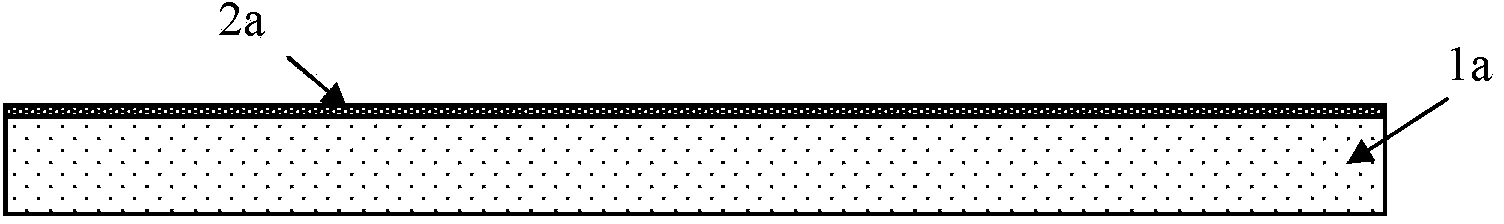
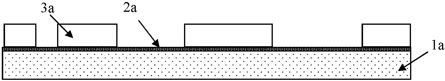
[0067] Step 1, such as Figure 16 As shown, a dielectric layer 1 is prepared first, and a conductive layer 2 of copper foil with Rz less than 4 μm is hot-pressed on the dielectric layer 1 . The dielectric layer 1 can be fabricated on a composite substrate including an insulating carrier and a surface conductive layer, or can be directly fabricated on a conductive layer. In this embodiment, the d...

Embodiment 2

[0079] The first step to the sixth step are the same as in Example 1.

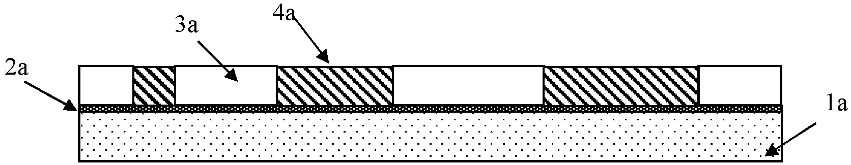
[0080] Step 7, see Figure 22 , continue to electroplate the substrate 3 containing the electroplating barrier layer 7, and then electroplate a layer of metal protective layer 10-bright nickel on the circuit pattern and the through hole, such as Figure 22 As shown, the metal protection layer 10 is electroplated bright nickel, and the thickness of the bright nickel is 3 μm.

[0081] Step 8, see Figure 23 , remove the plating stop layer 7.

[0082] Step 9, see Figure 24 , remove the exposed seed layer and the redundant copper foil conductive layer, retain the circuit pattern and the through hole 5, and form the required conductive pattern. The method of removing the bare seed layer and the conductive layer of copper foil adopts chemical etching. In this embodiment, the bare seed layer and the conductive layer are removed by flash etching, and the flash etching solution is a mixture of sulfuric acid a...

Embodiment 3

[0086] The first step to the sixth step are the same as in Example 1.

[0087] Step 7, see Figure 22 , the substrate 3 containing the electroplating barrier layer 7 is continued to be electroless plated, and a metal protection layer 10--silver is plated on the circuit pattern and the through hole again, such as Figure 22 As shown, the metal protective layer 10 is electroless plated silver, and the thickness of the silver is 0.15 μm.

[0088] Step 8, see Figure 23 , remove the plating stop layer 7.

[0089] Step 9, see Figure 24 , remove the exposed seed layer and redundant copper foil conductive layer, retain the circuit pattern and the through hole 5, and form the required circuit pattern. The method of removing the bare seed layer and the conductive layer of copper foil adopts chemical etching. In this embodiment, the bare seed layer and the copper foil conductive layer are removed by flash etching, and the flash etching solution is a mixture of sulfuric acid and hy...


PUM

PropertyMeasurementUnit
thicknessaaaaaaaaaa
surface roughnessaaaaaaaaaa
thicknessaaaaaaaaaa

Abstract

The invention relates to a method for manufacturing a printed circuit board by using a novel and improved semi-additive process. The method includes the following steps that: a) a dielectric layer is prepared, and copper foil is pressed on the dielectric layer, so that a copper foil conductive layer can be formed, and as a result, a composite structure substrate can be formed, the roughness of the rough surface of the copper foil being smaller than 4 microns; b) the thickness of the copper foil conductive layer is reduced to 0.2 to 5 microns; c) through holes or blind holes are formed in the dielectric layer and the copper foil conductive layer; d) conductive treatment is performed on the copper foil conductive layer and the hole walls of the blind holes or through holes, so that a seed layer can be formed; e) a photosensitive film is bonded on the surface of the substrate, and an electroplating barrier layer is formed on the substrate through pattern transfer; f) electroplating is performed on the substrate; g) a metal protective layer is formed on the surface of a circuit pattern through using a chemical plating or electroplating method; h) the electroplating barrier layer is removed; i) the bare seed layer and copper foil conductive layer are removed through adopting a flash rusting method, and the circuit pattern formed through electroplating is reserved; j) the metal protective layer is removed; and k) processing in steps from a) to j) is performed on the circuit board repeatedly, so that a multi-layer circuit board can be formed.

Description

technical field [0001] The invention relates to a method for manufacturing a printed circuit board, in particular to a method for manufacturing a printed circuit board (including an IC carrier board) by a novel and improved semi-additive method. Background technique [0002] With the development of electronic products in the direction of thinner and smaller, the requirements for product refinement are getting higher and higher. In the production of printed circuit boards, in addition to reducing the diameter of the via hole, reducing the size of the circuit is also an important direction to increase product density and reduce the size of the completed board. [0003] At present, in the circuit board manufacturing process, three typical pattern transfer technologies are: subtractive method, full additive method and semi-additive method. [0004] (1) subtraction method [0005] In the subtractive method, a photosensitive resist material is generally used to complete the patt...

Claims


Application Information

Patent Timeline
Patent Type & Authority Applications(China)
IPC IPC(8): H05K3/46H05K3/42
Inventor 付海涛罗永红赵丽程凡雄陈培峰
Owner SHANGHAI MEADVILLE SCI & TECH
Why Eureka
Try Eureka