Preparation method of transmission electron microscope sample

A transmission electron microscope sample and sample technology, which is applied in the field of integrated circuit manufacturing, can solve problems such as sample damage and electrical breakdown, and achieve the effect of avoiding accumulation and breakdown of the insulating layer

Active Publication Date: 2014-10-29
SHANGHAI HUALI MICROELECTRONICS CORP
View PDF6 Cites 18 Cited by
  • Summary
  • Abstract
  • Description
  • Claims
  • Application Information

AI Technical Summary

Problems solved by technology

[0004] However, it is clear to those skilled in the art that the current conventional method of using focused ion beams for TEM sample preparation sometimes causes electrical breakdown due to charge accumulation, such as figure 2 , figure 2 Schematic diagram of the structure of directly depositing a metal protective layer on the sample that needs to be cut and analyzed, figure 2 Among them, the surface of the silicon substrate 1 is an insulating layer 2, and a target st

Method used


Image

  • Preparation method of transmission electron microscope sample
  • Preparation method of transmission electron microscope sample
  • Preparation method of transmission electron microscope sample

Examples


Embodiment Construction

[0033] Attached below Figure 3-6 , the specific embodiment of the present invention will be further described in detail.

[0034] It should be noted that, in the following embodiments, the target structure in the form of trenches is taken as an example for illustration.

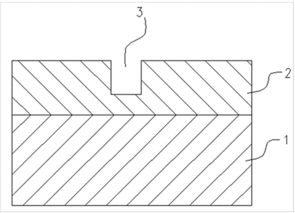
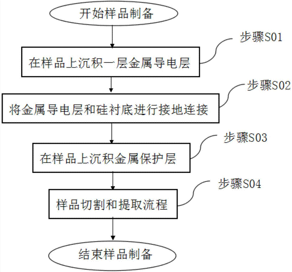
[0035] see image 3 , image 3 Make flow block diagram for sample of the present invention; It has illustrated a kind of preparation method of TEM sample, and described TEM sample comprises silicon substrate 1 and insulating layer 2, and described insulating layer 2 has target structure 3, and described target structure 3 is a through hole or a groove, and further includes the following steps:

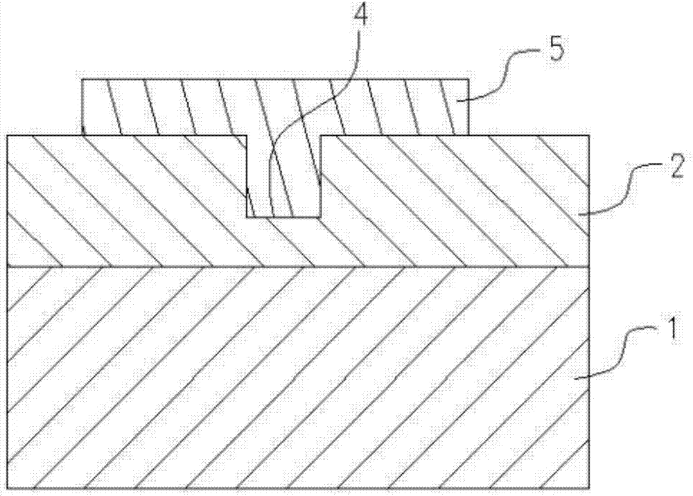
[0036] Step S01: depositing a metal conductive layer 6 on the surface of the sample and the inner wall of the target structure 3;

[0037] see Figure 4 , Figure 4 It is a structural schematic diagram of depositing a layer of metal conductive layer on the sample in the present invention. The deposition method ...


PUM

PropertyMeasurementUnit
Thicknessaaaaaaaaaa
Depthaaaaaaaaaa

Abstract

The invention discloses a preparation method of a transmission electron microscope sample. The transmission electron microscope sample comprises a silicon substrate and an insulating layer, wherein a through-hole or groove type target structure is formed on the insulating layer. The preparation method comprises the following steps: firstly, depositing a metal conductive layer on the surface of the insulating layer; connecting the metal conductive layer with the silicon substrate, wherein the sample is directly arranged on a sample table in a focused ion beam system and the silicon substrate is grounded through the sample table; and then depositing a metal protective layer on a target structure part on the metal conductive layer. During sample cutting, electric charges generated by the metal protective layer can be conducted to the silicon substrate and then grounded through the sample table, so that the charge accumulation in the target structure is avoided and the problem that the target structure is damaged by electric breakdown is prevented; according to the method, the problems such as the charge accumulation in the target structure and the breakdown of the insulating layer are avoided during the sample cutting, so that real and intact information of the target structure is obtained.

Description

technical field [0001] The invention relates to the technical field of integrated circuit manufacturing, in particular to a method for preparing a semiconductor integrated circuit transmission electron microscope sample. Background technique [0002] In the production process of integrated circuits, it is necessary to use TEM (transmission electron microscope) to observe various structures, such as the morphology of the first metal layer after etching. The morphology refers to the through holes or trenches formed during etching. Groove and other structures, the observation of this structure needs to cut the sample, such as figure 1 , figure 1 A schematic diagram of the sample structure that needs to be cut and analyzed, figure 1 Among them, the surface of the silicon substrate 1 is an insulating layer 2, and the target structure 3 is etched on the insulating layer 2. The silicon substrate 1 is generally several hundred μm (micrometer) thick. If the ion beam is directly use...

Claims


Application Information

Patent Timeline
IPC IPC(8): G01N1/28
Inventor 陈强
Owner SHANGHAI HUALI MICROELECTRONICS CORP
Why Eureka
Try Eureka