

Semiconductor device forming method
A semiconductor and device technology, applied in the field of semiconductor device formation, can solve the problems of expensive, time-consuming, repeated exposure steps, etc., and achieve the effect of reducing process difficulty and production cost, and reducing cost
- Summary
- Abstract
- Description
- Claims
- Application Information
AI Technical Summary
Problems solved by technology
Method used
Image

Examples
no. 1 example
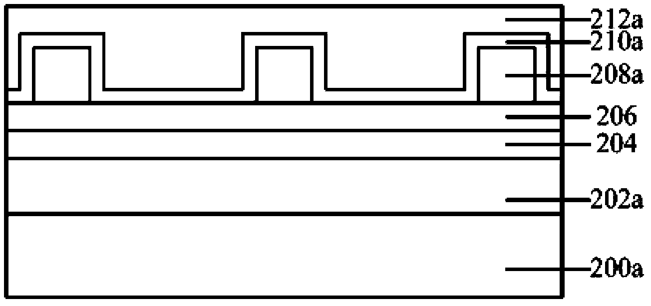
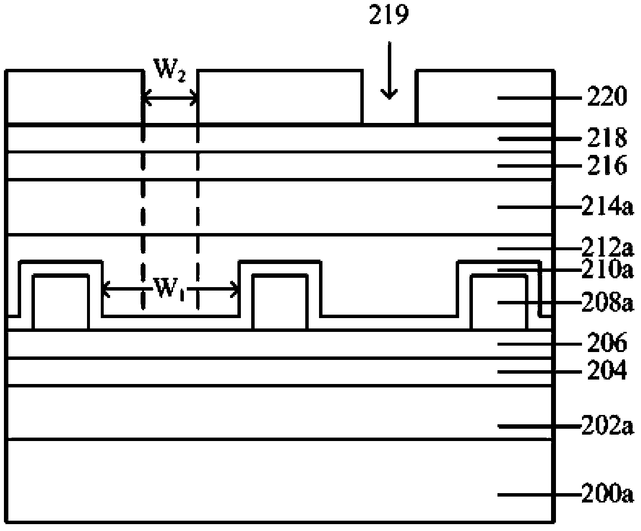
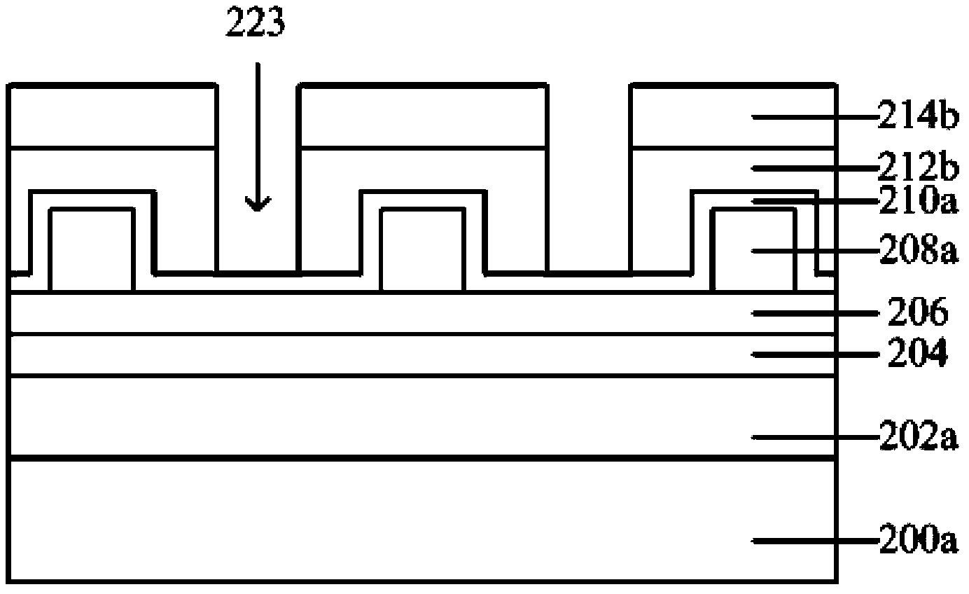
[0039] refer to figure 1 , providing a semiconductor substrate 200a, and forming a first mask layer on the semiconductor substrate 200a.
[0040] In this embodiment, the material of the semiconductor substrate 200a can be single crystal silicon, single crystal germanium or single crystal silicon germanium, silicon-on-insulator, III-V group element compounds, single crystal silicon carbide, etc. other materials.
[0041] In addition, a device structure (not shown in the figure) may also be formed in the semiconductor substrate 200a, and the device structure may be a device structure formed in a semiconductor front-end process, such as a MOS transistor.
[0042] In this embodiment, the first mask layer is a multi-layer structure, and forming the first mask layer on the semiconductor substrate 200a includes: sequentially forming an organic distribution layer 202a, a second mask layer on the semiconductor substrate 200a from bottom to top, Two hard mask layers 204, bottom anti-...
no. 2 example
[0081] refer to Figure 8 , providing a semiconductor substrate 300a, and forming a first mask layer on the semiconductor substrate 300a.
[0082] In this embodiment, the first mask layer is a multi-layer structure, and forming the first mask layer on the semiconductor substrate 300a includes: sequentially forming an organic distribution layer 302 on the semiconductor substrate 300a from bottom to top , a second hard mask layer 304 and a photoresist layer.
[0083] In this embodiment, please refer to the first embodiment for the structure and formation process of the semiconductor substrate 300 a , the organic distribution layer 302 , the second hard mask layer 304 and the photoresist layer, and details are not repeated here.
[0084] In another embodiment, after forming the second hard mask layer 304 and before forming the photoresist layer, forming a bottom anti-reflection layer on the second hard mask layer 304 may also be included. (not shown).
[0085] continue to refe...
PUM
| Property | Measurement | Unit |
|---|---|---|
| Thickness | aaaaa | aaaaa |
| Thickness | aaaaa | aaaaa |
| Thickness | aaaaa | aaaaa |
Abstract
Description
Claims
Application Information