Substrate chip carrier CSP package and production method thereof
A technology of substrate sheet type and manufacturing method, which is applied in the field of electronic device manufacturing and semiconductor packaging, and can solve problems such as large specific gravity, difficulty in accommodating dies, and high heat generation density of devices
- Summary
- Abstract
- Description
- Claims
- Application Information
AI Technical Summary
Problems solved by technology
Method used
Image

Examples
Embodiment 1
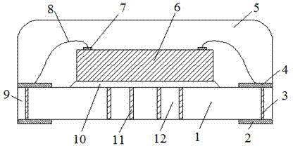
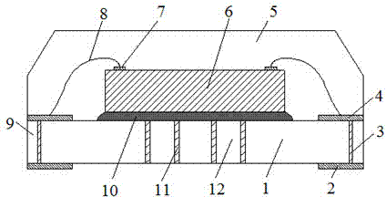
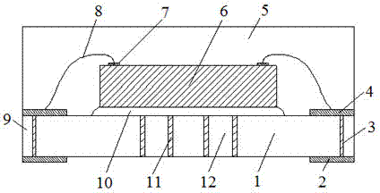
[0045] The surface of the wafer is thinned by the thinning process of coarse grinding + fine grinding + polishing; the thickness of the wafer after rough grinding is 350 μm, and the thickness of the wafer after fine grinding is 280 μm; polishing makes the surface roughness of the wafer reach 0.05 μm ~ 0.12 μm; the back of the thinned wafer is pasted with a blue film, baked, and then the wafer is cut into individual IC chips by a double-knife scribing process; when scribing, the depth of the first knife mark is the thickness of the thinned wafer 2 / 3 of the thickness; the second knife directly separates the wafer into individual IC chips, and leaves obvious knife marks on the blue film pasted on the back of the wafer, which cannot penetrate the blue film; send the substrate to On the loading table of the chip loader, the diced wafer is placed on the wafer workbench, and the glue writing system equipped with the core loader is used to draw glue on the die bonding area on the subst...
Embodiment 2
[0047] The surface of the wafer is thinned by the thinning process of coarse grinding + fine grinding + polishing; the thickness of the wafer after rough grinding is 360 μm, and the thickness of the wafer after fine grinding is 290 μm; the polishing process makes the surface roughness of the wafer reach 0.05-0.12 μm; paste the blue film on the back of the thinned wafer, bake, and cut the wafer into individual IC chips by double-knife scribing process; when scribing, the depth of the first knife mark is the thinned wafer 2 / 3 of the thickness, the second knife directly separates the wafer into individual IC chips, and leaves obvious knife marks on the blue film pasted on the back of the wafer, and the blue film cannot be scratched through; send the substrate to the The loading table of the core machine, the diced wafer is placed on the wafer workbench, and the glue writing system equipped with the core loader is used to draw glue on the die bonding area on the substrate, and the ...
Embodiment 3
[0049]The thinning process of rough grinding + fine grinding + polishing is used to thin the wafer surface. The thickness of the wafer after rough grinding is 340 μm, and the thickness of the wafer after fine grinding is 270 μm; polishing makes the surface roughness of the wafer reach 0.05 μm ~ 0.12 μm; paste the blue film on the back of the thinned wafer, bake, and cut the wafer into individual IC chips by double-knife scribing process; when scribing, the depth of the first knife mark is the thinned wafer 2 / 3 of the thickness, the second knife directly separates the wafer into individual IC chips, and leaves obvious knife marks on the blue film pasted on the back of the wafer, and the blue film cannot be scratched through; send the substrate to the On the loading table of the core machine, place the diced wafer on the wafer workbench, use the adhesive writing system equipped with the core loader to draw glue on the die bonding area on the substrate, and use the thimble to lift...
PUM
 Abstract
Description
Claims
Application Information