Germanium-silicon heterojunction bipolar transistor single event effect resisting strengthening method based on simulation

A heterojunction bipolar, single-event effect technology, applied in semiconductor/solid-state device testing/measurement, special data processing applications, instruments, etc., can solve the problems of high production and trial production costs, long design and reinforcement cycles, etc., and achieve layout layout Improvement, save test funds and time, and ensure the effect of accuracy

Inactive Publication Date: 2014-11-05
XINJIANG TECHN INST OF PHYSICS & CHEM CHINESE ACAD OF SCI
View PDF4 Cites 3 Cited by
  • Summary
  • Abstract
  • Description
  • Claims
  • Application Information

AI Technical Summary

Problems solved by technology

These reinforcement technologies often need to change the process flow, the co

Method used


Image

  • Germanium-silicon heterojunction bipolar transistor single event effect resisting strengthening method based on simulation
  • Germanium-silicon heterojunction bipolar transistor single event effect resisting strengthening method based on simulation
  • Germanium-silicon heterojunction bipolar transistor single event effect resisting strengthening method based on simulation

Examples


Embodiment

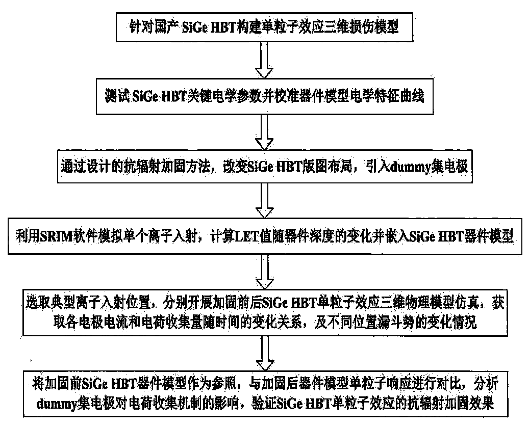
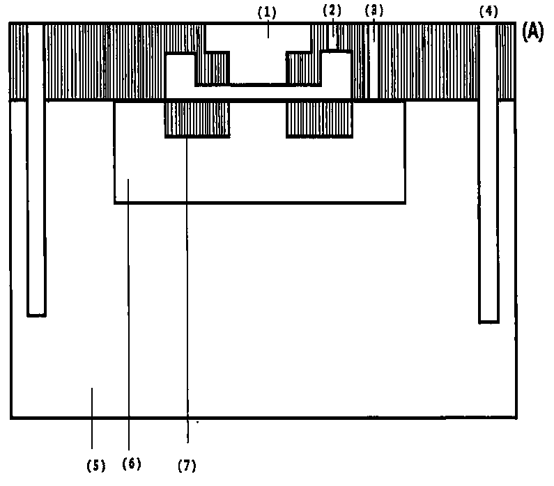
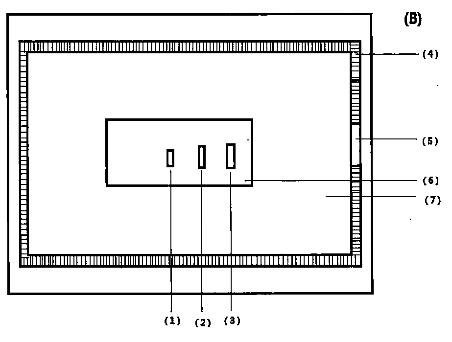
[0041] a. Construct a three-dimensional damage device model of germanium-silicon heterojunction bipolar transistor single event effect, select the internal geometric structure, regional material, and doping distribution of germanium-silicon heterojunction bipolar transistor (developed by Tsinghua University), and construct a reasonable grid And a complete device model, use the three-dimensional modeling editing language to write various parameters of the device structure, wherein the material of the emission area is polysilicon, and the three-dimensional structure size is X1=-0.2, X2=0.2, Y1=-0.17, Y2=0.17, Z1 =15, Z2=21, the doping concentration reaches 5e19cm-3; the base material is SiGe with gradient composition, and the three-dimensional structure size is X1=-0.8, X2=0.8, Y1=-0.08, Y2=0.0, Z1=12 , Z2=24, the doping concentration reaches 1e19cm-3; the collector material is N-type silicon, and the three-dimensional structure size is X1=-9, X2=9, Y1=-0.0, Y2=0.89, Z1=5, Z2=31 ...


PUM


Abstract

The invention relates to a germanium-silicon heterojunction bipolar transistor single event effect resisting strengthening method based on simulation. The method comprises the steps that a three-dimensional damage model is built, key electrical parameters of the model are calibrated, through the designed radiation resisting strengthening method, a device collector-substrate junction is extended, a fake collector is introduced, a single ion incident device is simulated through SRIM software, the change of a linear energy transmission value along with the device depth is obtained, a linear energy transmission value file is compiled, a device model is embedded, the typical incident position of ions is selected, single event effect simulation of a strengthened device model and single event effect simulation of a non-strengthened device model are carried out respectively, the device model obtained before strengthening is adopted as the reference and is compared with the single event response of the strengthened device model, and the radiation resisting strengthening effect of a germanium-silicon heterojunction bipolar transistor is verified. According to the method, the problems that a ground simulation test cost is high and the machine hour is tense are solved; the single event effect resisting capacity of the germanium-silicon heterojunction bipolar transistor is effectively improved, and meanwhile the defects that the process experiment cost is high and the period is long are overcome.

Description

technical field [0001] The invention relates to a semiconductor device anti-single event effect reinforcement method, in particular to a simulation-based anti-single event effect reinforcement method, which belongs to the technical field of microelectronics and the field of anti-radiation reinforcement technology. Background technique [0002] Semiconductor process and device simulation tool (TCAD) is an effective means to simulate semiconductor process conditions and device layout structure through computer simulation technology. With the continuous development of the research on the radiation effect of semiconductor devices, the computer simulation method that combines device simulation tools with particle transport simulation calculations has solved the problems of high cost and short machine time for ground simulation tests, and can make up for the high cost of process experiments And the shortcoming of long cycle. [0003] Single Event Effects (SEE) are microelectronic...

Claims


Application Information

Patent Timeline
IPC IPC(8): G06F17/50H01L21/66
Inventor 郭红霞郭旗李培文林王信刘默寒崔江维陆妩余学峰何承发
Owner XINJIANG TECHN INST OF PHYSICS & CHEM CHINESE ACAD OF SCI
Why Eureka
Try Eureka