Flash memory unit and formation method thereof

A technology of flash memory storage and floating gate, which is applied in the direction of electrical components, transistors, electric solid-state devices, etc., and can solve the problems of high difficulty in size reduction and large size of flash memory storage cells, so as to reduce overlapping area, area reduction, and size reduction Effect

Active Publication Date: 2014-11-19
SHANGHAI HUAHONG GRACE SEMICON MFG CORP
View PDF4 Cites 6 Cited by
  • Summary
  • Abstract
  • Description
  • Claims
  • Application Information

AI Technical Summary

Problems solved by technology

[0004] However, the size of the existing flash memory storage

Method used


Image

  • Flash memory unit and formation method thereof
  • Flash memory unit and formation method thereof
  • Flash memory unit and formation method thereof

Examples


Embodiment Construction

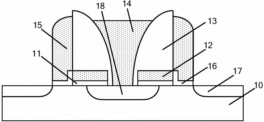
[0023] As mentioned in the background, the size of the existing flash storage unit is relatively large, and it is difficult to further reduce the size.

[0024] After research, please refer to figure 1 , when the flash memory cell is working, a channel region is formed between the source line doped region 18 and the bit line doped region 17, and the floating gate 12 is biased through the source line doped region 18, which can Carriers are controlled to migrate between the channel region and the floating gate 12 through the tunnel oxide layer 11 . However, if figure 1 In the shown flash storage unit, in order to apply a bias voltage to the floating gate 12, it is necessary to have an overlapping region between the source line doped region 18 and the floating gate 12, and the source line doped region 18 An applied bias voltage can be coupled to the floating gate 12 such that the floating gate 12 is biased, thus controlling the tunneling of hot carriers. Moreover, the larger t...


PUM

PropertyMeasurementUnit
Lengthaaaaaaaaaa
Lengthaaaaaaaaaa
Lengthaaaaaaaaaa

Abstract

The invention discloses a flash memory unit and a formation method thereof. The flash memory unit comprises a substrate, a floating gate, a source line doping area, a second dielectric layer, a control gate, a first side wall, a third dielectric layer, word lines and a bit line doping area, wherein the surface of the substrate is provided with a first dielectric layer, the floating gate is located on the surface of the first dielectric layer, a second opening is formed inside the floating gate, the source line doping area is located at the position, at the bottom of the second opening, inside the substrate, the second dielectric layer is located on the surface of the floating gate and arranged on the surface of the position, at the bottom of the second opening, of the substrate, the control gate is located on the surface of the second dielectric layer, the first side wall is located on the surface of the side wall of the control gate, the third dielectric layer is located on the surface of the side wall of the floating gate, the word lines are located on the two sides of the first side wall, the two sides of the control gate, the two sides of the floating gate and the two sides of the third dielectric layer, and the bit line doping area is located inside the position, on the two sides of the first side wall, the two sides of the control gate, the two sides of the floating gate and the two sides of the word lines, of the substrate. The size of the formed flash memory unit is reduced.

Description

technical field [0001] The invention relates to the technical field of semiconductor manufacturing, in particular to a flash memory storage unit and a forming method thereof. Background technique [0002] In the current semiconductor industry, integrated circuit products can be mainly divided into three types: analog circuits, digital circuits and digital / analog hybrid circuits, among which storage devices are an important type of digital circuits. In recent years, among storage devices, flash memory (flash memory) has developed particularly rapidly. The main feature of flash memory is that it can keep stored information for a long time without power on; and it has the advantages of high integration, fast access speed, easy erasing and rewriting, etc., so it has been widely used in many fields such as microcomputer and automatic control. a wide range of applications. [0003] figure 1 It is a schematic cross-sectional structure diagram of an existing flash storage unit, i...

Claims


Application Information

Patent Timeline
IPC IPC(8): H01L21/8247H01L27/115H01L29/423H01L29/788
CPCH10B41/00H10B41/30
Inventor 于涛肖军
Owner SHANGHAI HUAHONG GRACE SEMICON MFG CORP
Why Eureka
Try Eureka