N-channel field effect transistor resistant to single particle effect and manufacturing method thereof

An anti-single event effect, transistor technology, applied in semiconductor/solid-state device manufacturing, electric solid-state devices, semiconductor devices, etc., can solve problems such as increasing circuit response time, reduce transient current pulse time and peak value, and improve resistance The effect of reduction in irradiation capacity, charge amount and absorption time

Active Publication Date: 2014-11-19
XIANGTAN UNIV
View PDF3 Cites 5 Cited by
  • Summary
  • Abstract
  • Description
  • Claims
  • Application Information

AI Technical Summary

Problems solved by technology

[0004] The hardening methods for single event transients can be divided into two types: device level hardening and circuit level hardening. The most common type of ci

Method used


Image

  • N-channel field effect transistor resistant to single particle effect and manufacturing method thereof
  • N-channel field effect transistor resistant to single particle effect and manufacturing method thereof
  • N-channel field effect transistor resistant to single particle effect and manufacturing method thereof

Examples


Embodiment Construction

[0015] The present invention will be described in detail below in conjunction with the accompanying drawings and embodiments.

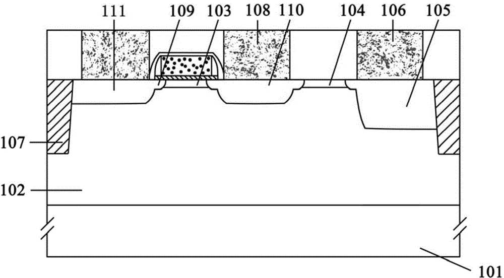
[0016] Such as figure 1 as shown, figure 1 It is a schematic cross-sectional structure diagram of an N-channel field-effect transistor resistant to single event effect of the present invention. 101 is a heavily doped substrate; the epitaxial layer 102 is grown on the substrate 101; on the epitaxial layer 102, the drain region 110 and the source region 111 are located at both ends; the first threshold voltage injection region 103 is located at the drain region 110 and the source region 111, on which is the gate oxide layer and the gate; the drain region electrode 108 is connected to the drain region 110, and connected to the voltage V DD The deep doped drain region 105 is located on the epitaxial layer 102, on the right side of the drain region 110; between the deeply doped drain region 105 and the drain region 110 is the second threshold voltage inj...


PUM

PropertyMeasurementUnit
Thicknessaaaaaaaaaa

Abstract

The invention discloses an N-channel field effect transistor resistant to the single particle effect and a manufacturing method of the N-channel field effect transistor. The N-channel field effect transistor resistant to single particle effect comprises a semiconductor substrate, an epitaxial layer, a source region, a drain region and a grid electrode. A first threshold voltage injection region is arranged between the source region and the drain region. The periphery of the drain region is provided with a deep doping leakage region. A second threshold voltage injection region is arranged between the deep doping leakage region and the drain region. According to the N-channel field effect transistor resistant to single particle effect and the manufacturing method of the N-channel field effect transistor, a circle of the deep doping leakage region surrounds the periphery of the drain region of a traditional N-channel field effect transistor, and the additionally arranged deep doping leakage region can effectively assist the drain region in collecting electric charge after single particle conducts incidence on the sensitive drain region and generates the funneling effect, so that quantity of electric charge absorbed by the drain region and the absorbing time are reduced after the drain region is irradiated by the single particle, the single particle transient current pulse time and peak are reduced, certain transient voltage pulse generated by the single particle with the linear energy transfer value in an inverter chain, and irradiation resistance of a device is improved.

Description

technical field [0001] The invention relates to integrated circuit technology, in particular to an anti-single event effect N-channel field-effect transistor with anti-radiation capability and a manufacturing method thereof. Background technique [0002] Radiation will have a serious impact on the performance of integrated circuits, and the radiation environment mainly causes two effects on integrated circuits: total dose effect and single event effect. With the advancement of microelectronics technology, the feature size of devices is getting smaller and smaller, the impact of total dose effect on integrated circuits has become weaker and weaker, while the impact of single event effect is increasing. [0003] The single event effect means that when a single high-energy particle penetrates the sensitive area of ​​an electronic device, it causes ionization and deposits charges on its trajectory. These deposited charges are collected by the sensitive area, causing the logic st...

Claims


Application Information

Patent Timeline
IPC IPC(8): H01L27/105H01L29/78H01L21/8238H01L21/76
Inventor 唐明华徐新宇燕少安张万里
Owner XIANGTAN UNIV
Why Eureka
Try Eureka