Solid-state electronic switch with characteristic of conversion from normally-open state to normally-closed state and preparation method thereof

An electronic switch and state conversion technology, applied in electronic switches, electrical components, pulse technology, etc., can solve the problems of mechanical shock and temperature shock sensitivity, low yield of structural adhesion, unstable switch structure, etc., and achieve the voltage signal amplitude. Large, excellent anti-static and electromagnetic interference, low power consumption effect

Inactive Publication Date: 2014-11-26
BEIJING INSTITUTE OF TECHNOLOGYGY
View PDF3 Cites 2 Cited by
  • Summary
  • Abstract
  • Description
  • Claims
  • Application Information

AI Technical Summary

Problems solved by technology

This type of switch can reduce the influence of external electromagnetic shock on its work to a certain extent, and can achieve bidirectional conduction, but it is more sensitive to mechanical shock and temperature shock
Because it contains moving parts, the electrical connection through the moving parts makes the switch structure unstable, and it is easy to produce structural adhesion during the process of micromachining and releasing, resulting in low yield. At the same time, the moving parts are difficult to meet certain requirements. The need for use after long-term storage
Also, most MEMS switches are not bistable
In addition, due to manufacturing process issues, this type of switch is also difficult to be compatible with mature integrated circuit semiconductor processes

Method used


Image

  • Solid-state electronic switch with characteristic of conversion from normally-open state to normally-closed state and preparation method thereof
  • Solid-state electronic switch with characteristic of conversion from normally-open state to normally-closed state and preparation method thereof
  • Solid-state electronic switch with characteristic of conversion from normally-open state to normally-closed state and preparation method thereof

Examples


Embodiment 1

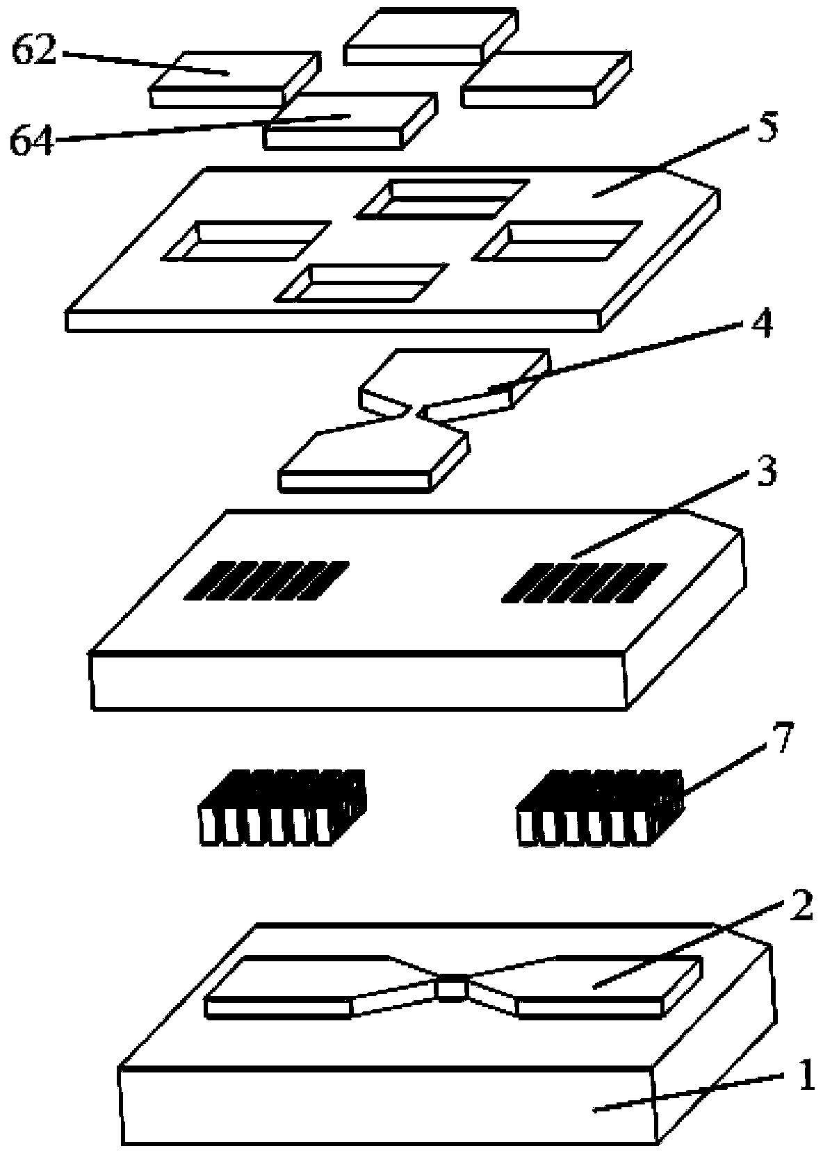
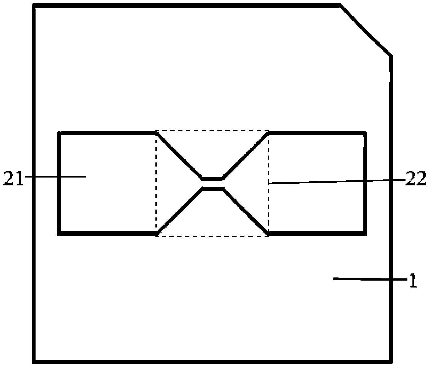
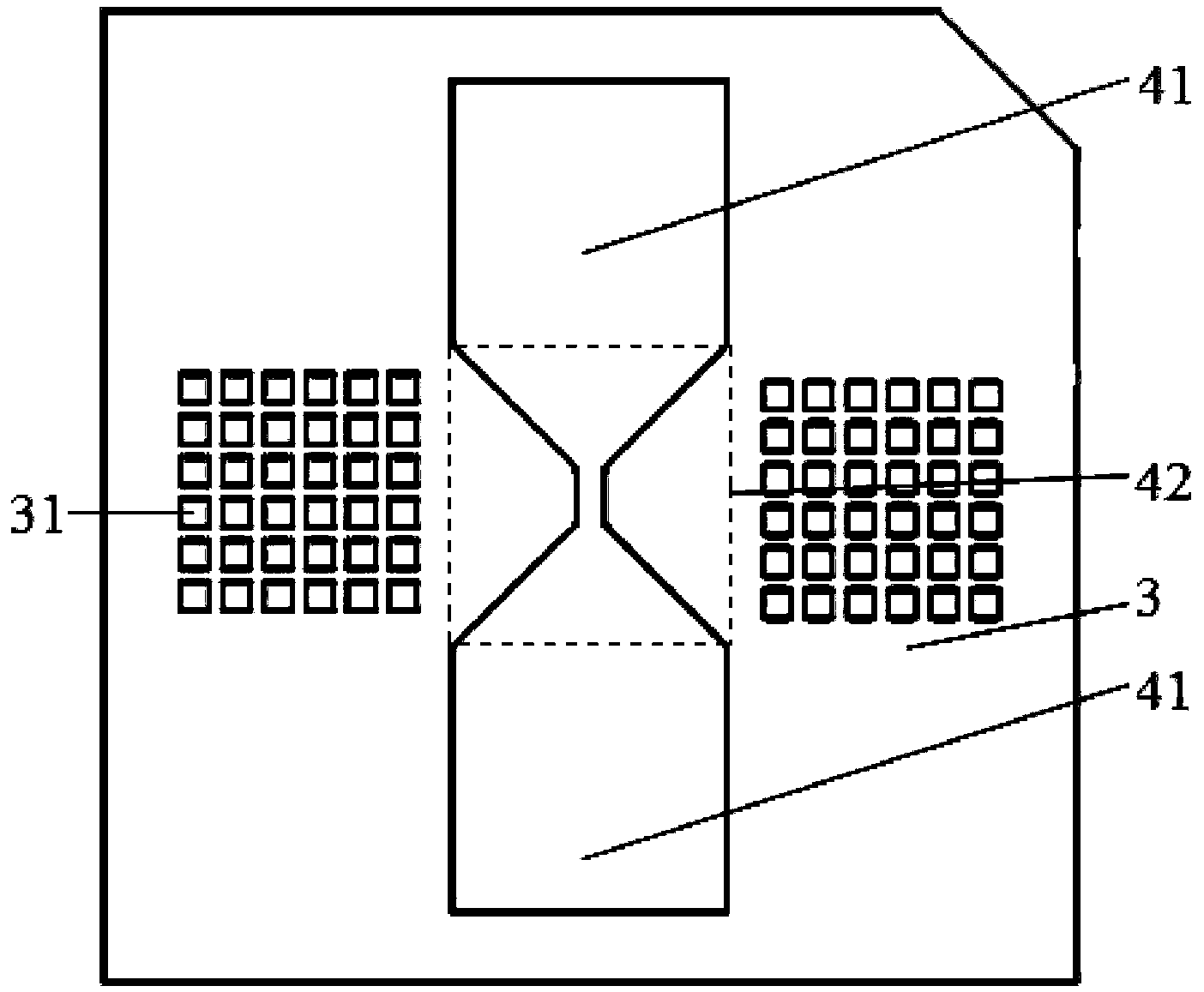
[0047] Such as figure 1 As shown, the solid-state electronic switch from normally-on to normally-off state of this embodiment includes: substrate 1, control bridge 2, insulating layer 3, controlled bridge 4, passivation layer 5, metal interconnection 7, a pair of control An electrode pad 62 and a pair of controlled electrode pads 64; wherein, the control bridge 2 is formed on the substrate 1, including a pair of control electrodes 21, and a control bridge region 22 connecting the two; the insulating layer 3 covers the control bridge 2; on the insulating layer 3, a plurality of through holes 31 are arranged at the position facing the pair of control electrodes 21 of the control bridge 2, forming a through hole array; the controlled bridge 4 is formed on the insulating layer 3, including a pair of controlled Electrode 41, and the controlled bridge area 42 that connects the two; The shape of control bridge 2 and controlled bridge 4 is a symmetrical figure, and the symmetrical axe...

Embodiment 2

[0051] Such as Figure 4 As shown, in this embodiment, the shape of the control bridge region 22 is rectangular, the length is not more than 40 μm, and the width is between 2-40 μm. The shape of the controlled bridge area 42 is similar to the shape of the controlled bridge area, as Figure 5 shown.

[0052] Taking Embodiment 2 as an example, the preparation method of the one-time bistable state of the present invention is converted from a normally-on to a normally-off state, comprising the following steps, such as Image 6 Shown:

[0053] S1. Provide a substrate, the material is silicon or silicon ;

[0054] S2. Oxidizing the substrate;

[0055] S3. Cover the substrate with a layer of material for the control bridge by sputtering, chemical vapor deposition CVD, ion implantation, etc., with a thickness not exceeding 2 μm, and the material for the control bridge is Al;

[0056] S4. Pattern the material of the control bridge by photolithography and etching to form a control...


PUM


Abstract

The invention discloses a solid-state electronic switch with characteristic of conversion from a normally-open state to a normally-closed state and a preparation method thereof. The solid-state electronic switch consists of a substrate, a control bridge, an insulating layer, a metal interconnection unit, a controlled bridge, a passivation layer, a pair of control electrode welding pads and a pair of controlled electrode welding pads. The control bridge is connected to a control circuit by the pair of control electrode welding pads, thereby receiving a control signal from the control circuit; and the controlled bridge is connected to a controlled circuit by the pair of controlled electrode welding pads. According to the invention, the solid-state electronic switch only consumes the electric energy at the moment of state conversion and does not consume electric energy in states of connection maintaining and disconnection, so that the switch has the bistable state characteristic; bidirectional conduction can be realized and no movable component is contained, so that the switch can work in a severe environment; the switch has the excellent anti-statistic and anti-electromagnetic interface characteristics; on the basis of the semiconductor technology of the integrated circuit, the switch has the high compatibility with the semiconductor technology of the integrated circuit; and the switch can be used as the short-circuit safety switch of an electric explosive device.

Description

technical field [0001] The invention relates to a microcomputer electronic switch, in particular to a solid-state electronic switch for switching from a normally-on state to a normally-off state and a preparation method thereof. Background technique [0002] Microelectronic switches based on integrated circuit semiconductor technology mainly include diode switches and triode switches. These switches usually work in the saturation region or cut-off region and are not bistable, which means that continuous energy is required to maintain the switch on or off. supply. For a diode switch, when the voltage loaded on both ends of the PN node is higher than its withstand voltage, breakdown will occur, causing the switch tube to lose its switching function. For triode switches, the closing condition depends on the voltage difference between the emitter and the collector, so when the circuit is in a harsh environment, such as when the circuit power supply is difficult to provide a sta...

Claims


Application Information

Patent Timeline
Patent Type & Authority Applications(China)
IPC IPC(8): H03K17/56
Inventor 娄文忠丁旭冉赵越
Owner BEIJING INSTITUTE OF TECHNOLOGYGY
Why Eureka
Try Eureka