Method of manufacturing light emitting device

A technology of light-emitting device and light-emitting element, applied in chemical instruments and methods, optical elements, transportation and packaging, etc.

Inactive Publication Date: 2014-11-26
SAINT GOBAIN PERFORMANCE PLASTICS CORP
View PDF3 Cites 16 Cited by
  • Summary
  • Abstract
  • Description
  • Claims
  • Application Information

AI Technical Summary

Problems solved by technology

However, ETFE membranes are only available from a limited number of suppliers

Method used


Image

  • Method of manufacturing light emitting device
  • Method of manufacturing light emitting device
  • Method of manufacturing light emitting device

Examples


Embodiment Construction

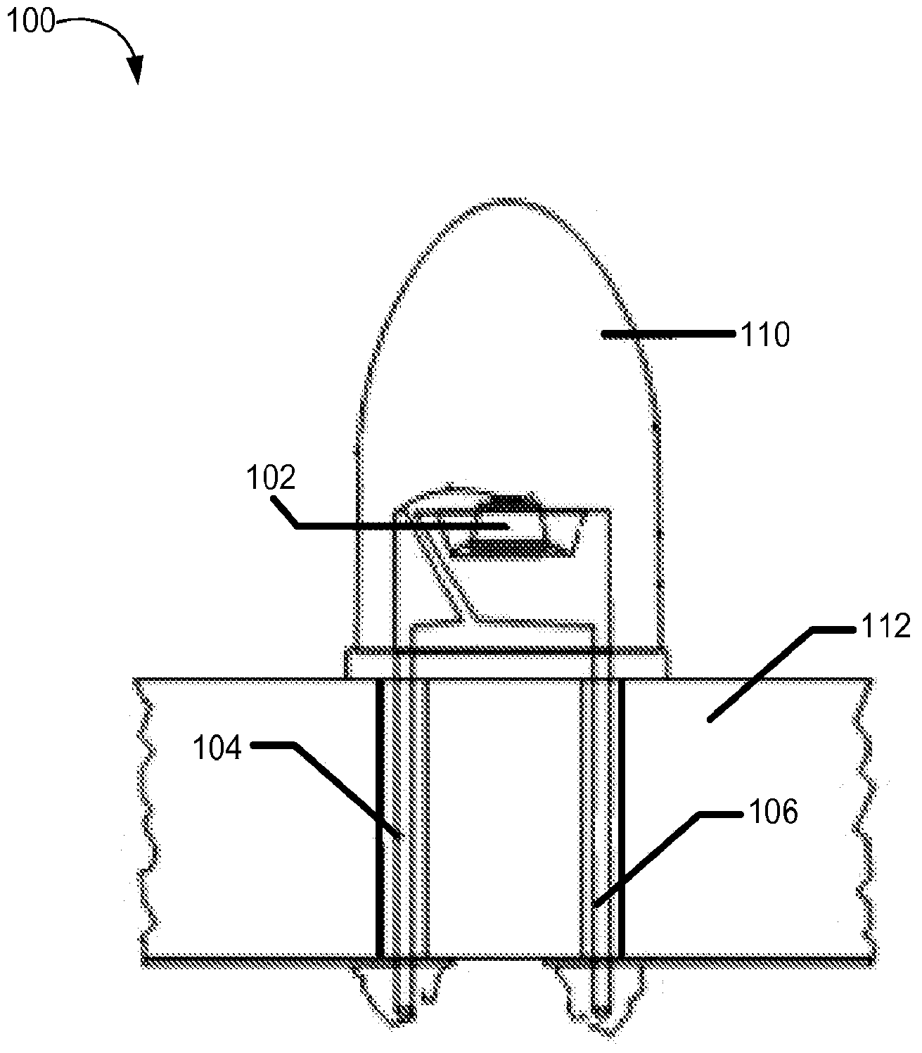
[0015] The preferred embodiment of the present invention relates to a novel method for preparing a packaged light-emitting device. A typical manufacturing process for LED devices involves encapsulating the LED itself within a dome-shaped lens of epoxy or silicone. The encapsulation material (also known as potting material) not only protects the LED from damage caused by moisture, shock, etc., the encapsulation material must also adequately transmit the desired wavelength of light. The degree to which light is transmitted by the encapsulant (lens) is an important consideration in selecting an encapsulation material. Unfortunately, due to the refractive index of the material and the degree of total internal reflection, a certain amount of light generated by the LED chip is always trapped within the encapsulation material. The trapped light disadvantageously reduces or alters the light output of the LED device.

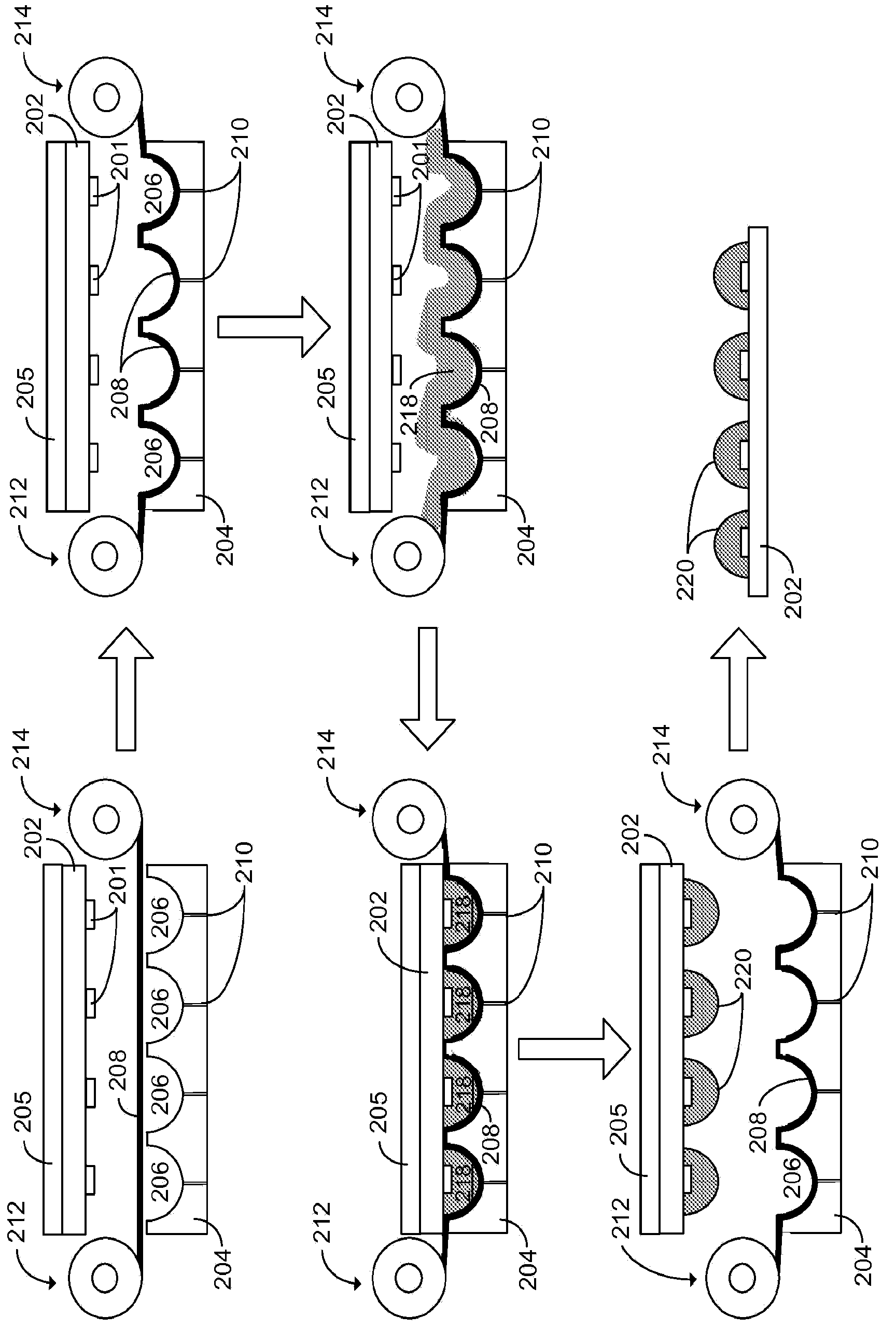
[0016] figure 2 A prior art method of forming an encapsulated L...


PUM

PropertyMeasurementUnit
elastic modulusaaaaaaaaaa

Abstract

A novel method of producing an encapsulated light emitting device. A preferred mold release film that can be used during the encapsulation of a LED chip has an elastic modulus and a glass transition temperature that are low enough as compared to the desired molding temperature that the release film will closely conform to the interior of the molding cavities used to form a protective lens surrounding an LED chip. A preferred release film according to embodiments of the present invention comprises a fully fluorinated polymer, such as a perfluoroalkoxy polymer, including MFA, or fluorinated ethylene propylene.

Description

technical field [0001] The present invention relates to the manufacture of light emitting devices, and more particularly to the use of release films in the manufacture of encapsulated light emitting diodes. Background technique [0002] Light emitting diodes (LEDs) are solid state semiconductor light sources that have several advantages over the more conventional incandescent light bulbs and fluorescent lamps. Some of the advantages of LEDs include low power consumption, small size, faster on / off time, low heat radiation, long useful life, impact resistance, and simple manufacturing process. Driven in part by the use of LED devices in new applications, the manufacture of LED devices continues to increase with increasing demand. [0003] Conventional LEDs generally include a semiconductor chip, an encapsulant, usually made of epoxy or silicone, and an electrical connection element comprising two metal leads bonded to contacts and connected to two metal leads emerging from th...

Claims


Application Information

Patent Timeline
Patent Type & Authority Applications(China)
IPC IPC(8): H01L33/48
CPCB29C2045/0075B29C2045/1477H01L33/54B29C2045/14155B29C45/14016H01L2933/005B29L2011/0016B29C45/14639B29D11/00807B29C33/62B29C33/68B29C37/0075B29C39/006H01L2924/181H01L24/97H01L2224/48091H01L2224/48247H01L2224/45144Y10T428/24355H01L2924/00012H01L2924/00014H01L2924/00B32B27/32H01L33/48H01L33/52H01L25/0753C08J5/18B29L2031/34C08J2329/10C08J2327/18C08J2327/20
Inventor D·伯拉维特M·A·亚当科
Owner SAINT GOBAIN PERFORMANCE PLASTICS CORP
Why Eureka
Try Eureka