Method for restoration of dielectric K value

A technology for repairing medium and K value, which is applied in the fields of electrical components, semiconductor/solid-state device manufacturing, circuits, etc. It can solve the problems of easily damaged media and achieve the effect of repairing K value

Active Publication Date: 2014-12-03
SEMICON MFG INT (SHANGHAI) CORP
View PDF7 Cites 0 Cited by
  • Summary
  • Abstract
  • Description
  • Claims
  • Application Information

AI Technical Summary

Problems solved by technology

[0006] In view of the shortcomings of the prior art described above, the purpose of the present invention is to provide a method for repairing the K value of the medium, which is used to solve the problem that the repair method in the prior art is easy to damage the medium

Method used


Image

  • Method for restoration of dielectric K value
  • Method for restoration of dielectric K value
  • Method for restoration of dielectric K value

Examples


Embodiment 1

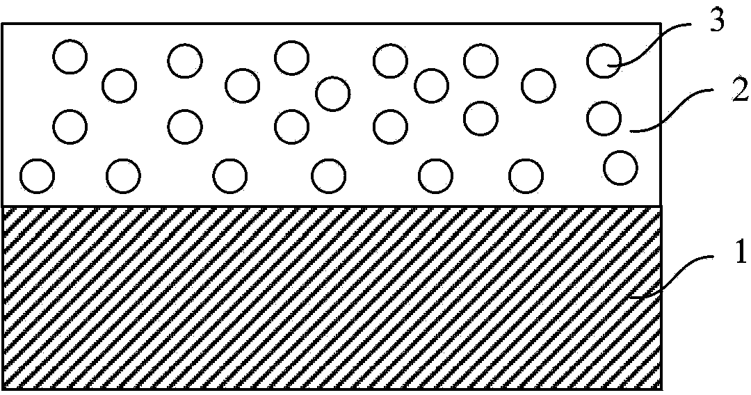
[0039] see Figure 1 to Figure 5 , the present invention provides a method for repairing the K value of a medium, the method for repairing the K value of a medium at least comprises the following steps:

[0040] Step 1), first see figure 1 , a substrate 1 is provided, and a dielectric layer 2 is formed on the substrate 1;

[0041] Specifically, the substrate 1 may be a conventional semiconductor substrate such as Si, Ge, SOI, etc., or may be a laminated structure including some devices. The medium layer 2 is a low-K medium. In this embodiment, the medium layer 2 is preferably a porous ultra-low-K medium; the porous ultra-low-K medium satisfies Kfigure 1 A number of holes 3 in the dielectric layer 2 are shown in FIG. In this embodiment, the dielectric layer 2 is formed by chemical vapor deposition on the substrate 1 firstly to form a dielectric film layer, and then a number of holes 3 are formed in the dielectric film layer by porogen and ultraviolet light treatment. It shou...

Embodiment 2

[0055] Embodiment 2 adopts basically the same solution as Embodiment 1, except that in Embodiment 2, the step of irradiating the dielectric layer with microwaves is further included after the polishing process in the subsequent process flow.

[0056] see Figures 6 to 8 , the present invention provides a method for repairing the K value of a medium, the method for repairing the K value of a medium at least comprises the following steps:

[0057] Step 1), providing a substrate, and forming a dielectric layer on the substrate;

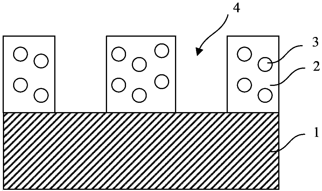
[0058] Step 2), etching a number of grooves in the dielectric layer, and cleaning to remove etching residues;

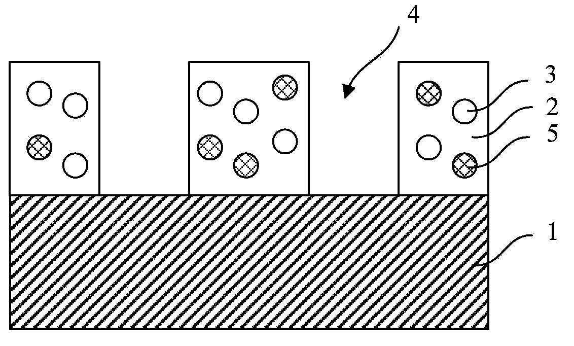
[0059] Step 3), using microwave to irradiate the etched dielectric layer.

[0060] It should be pointed out that the steps 1) to 3) in this embodiment are the same as the steps 1) to 3) in Figure 1 to Figure 5 and related text descriptions, which will not be repeated here.

[0061] Then proceed to step 4), see Image 6 , Fill metal 6 in t...


PUM

PropertyMeasurementUnit
wavelengthaaaaaaaaaa

Abstract

The invention provides a method for restoration of a dielectric K value. The method at least includes the following steps: 1) providing a substrate and forming a dielectric layer on the substrate; 2) etching a plurality of grooves in the dielectric layer and cleaning and removing etching residues; 3) adopting microwaves to irradiate the dielectric layer which undergoes the etching. The method for restoration of the dielectric K value makes use of strong microwave-absorbing property of water to remove moisture in the dielectric layer so as to restore the K value of the dielectric layer; and that the energy gap of the dielectric layer is far larger than photon energy of the microwaves is used so that the microwaves are not absorbed and a problem of damage of the dielectric layer is prevented.

Description

technical field [0001] The invention belongs to the field of semiconductor manufacturing, and relates to a method for processing a dielectric layer, in particular to a method for restoring the K value of a dielectric. Background technique [0002] With the rapid development of integrated circuit CMOS technology in accordance with Moore's Law, interconnect delay has gradually replaced device delay as a key factor affecting chip performance. Parasitic capacitances and interconnect resistances between interconnects cause signal propagation delays. Since copper has lower resistivity, superior anti-electromigration properties and high reliability, it can reduce the interconnect resistance of the metal, thereby reducing the overall interconnect delay effect, which has been changed from conventional aluminum interconnects to low Resistive copper interconnects. At the same time, reducing the capacitance between interconnects can also reduce the delay, and the parasitic capacitance...

Claims


Application Information

Patent Timeline
Patent Type & Authority Applications(China)
IPC IPC(8): H01L21/768H01L21/3105
CPCH01L21/76825H01L21/76826
Inventor 王宗涛周鸣
Owner SEMICON MFG INT (SHANGHAI) CORP
Why Eureka
Try Eureka