Organic light-emitting device and preparation method thereof

An electroluminescence device and electroluminescence technology, which are applied in the directions of organic semiconductor devices, materials of organic semiconductor devices, and electric solid devices, etc., and can solve the problems of no bending, fragile glass, poor mechanical strength, etc.

Inactive Publication Date: 2014-12-03
OCEANS KING LIGHTING SCI&TECH CO LTD +2
View PDF6 Cites 4 Cited by
  • Summary
  • Abstract
  • Description
  • Claims
  • Application Information

AI Technical Summary

Problems solved by technology

[0003] Among OLED devices in the prior art, OLED devices made of glass substrates do not have the characteristics of bending, and the glass is fragile, which affects the application of light emitting devices
Stainless steel sheet can be used as a substrate material for flexible devices, but due to its large surface roughness, it is prone to fall off, thus destroying the entire OLED device and affecting the stability of light emission
For flexible OLED products, if traditional OLED packaging technology is used, adding a packaging cover on the back of the device will cause problems such as heavy weight, high cost, and poor mechanical strength, which will limit the performance of flexible OLED products.
At present, most flexible OLEDs are not waterproof and oxygen-resistant, and have a short service life. The preparation process is complicated and the cost is high.

Method used


Image

  • Organic light-emitting device and preparation method thereof
  • Organic light-emitting device and preparation method thereof
  • Organic light-emitting device and preparation method thereof

Examples


Embodiment 1

[0101] A method for preparing an organic electroluminescent device, comprising the following steps:

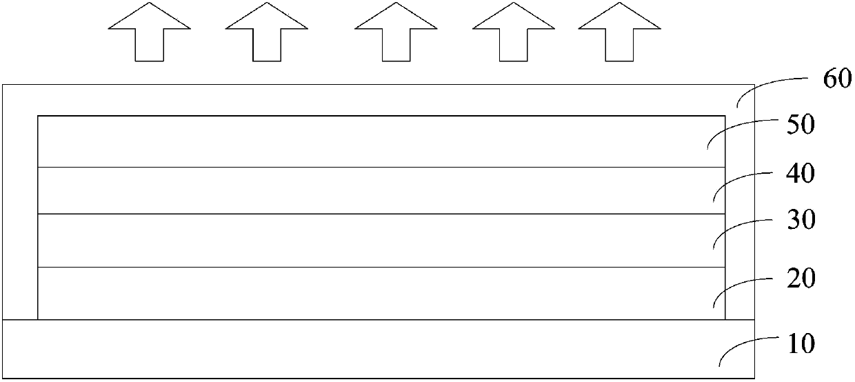
[0102] (1) Provide a stainless steel sheet with a thickness of 0.05mm as the substrate;

[0103] (2) Prepare a buffer layer on the substrate:

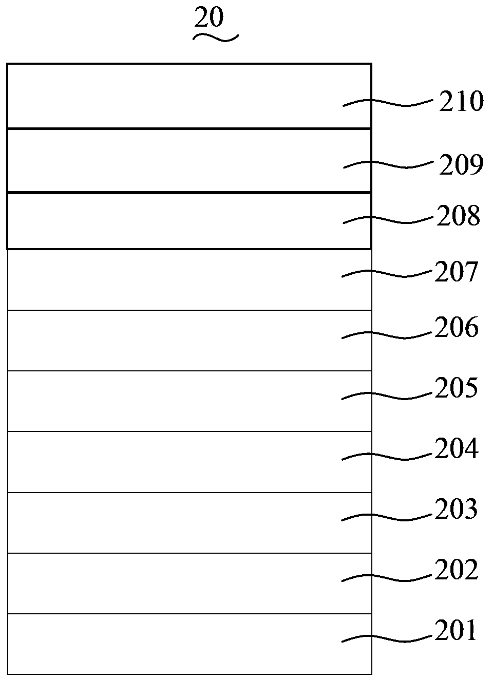
[0104] a. Get the solid p-xylene ring dimer, sublimate to gaseous state at 170°C, then crack at 690°C to obtain the gaseous monomer molecules of p-xylene with free radicals;

[0105] b. The substrate is placed in a vacuum deposition chamber, gaseous monomer molecules are introduced, and the gaseous monomer molecules are polymerized on the substrate to form a parylene film;

[0106] c. At a vacuum of 5×10 -4 In the sputter coating chamber of Pa, silicon dioxide film was prepared by sputtering on the parylene film, the sputtering conditions were acceleration voltage 500V, magnetic field 100G, power density 20W / cm 2 ;

[0107] Repeat steps a to c for a total of 5 times to prepare a buffer layer;

[0108] (3) In a vacuum of 5×10 -4 I...

Embodiment 2

[0120] A method for preparing an organic electroluminescent device, comprising the following steps:

[0121] (1) Provide a stainless steel sheet with a thickness of 0.1mm as the substrate;

[0122] (2) Prepare a buffer layer on the substrate:

[0123] a. Get the solid p-xylene ring dimer, sublimate to gaseous state at 170°C, then crack at 690°C to obtain the gaseous monomer molecules of p-xylene with free radicals;

[0124] b. The substrate is placed in a vacuum deposition chamber, gaseous monomer molecules are introduced, and the gaseous monomer molecules are polymerized on the substrate to form a parylene film;

[0125] c. At a vacuum of 1×10 -5 In the sputter coating chamber of Pa, silicon dioxide film was prepared by sputtering on the parylene film, the sputtering conditions were acceleration voltage 300V, magnetic field 50G, power density 1W / cm 2 ;

[0126] Repeat steps a to c for a total of 6 times to prepare a buffer layer;

[0127] (3) In a vacuum of 1×10 -5 In t...

Embodiment 3

[0136] A method for preparing an organic electroluminescent device, comprising the following steps:

[0137] (1) Provide a stainless steel sheet with a thickness of 0.05mm as the substrate;

[0138] (2) Prepare a buffer layer on the substrate:

[0139] a. Get the solid p-xylene ring dimer, sublimate to gaseous state at 170°C, then crack at 690°C to obtain the gaseous monomer molecules of p-xylene with free radicals;

[0140] b. The substrate is placed in a vacuum deposition chamber, gaseous monomer molecules are introduced, and the gaseous monomer molecules are polymerized on the substrate to form a parylene film;

[0141] c. At a vacuum of 1×10 -3 In the sputtering coating chamber of Pa, aluminum oxide film was prepared by sputtering on the parylene film, the sputtering conditions were acceleration voltage 800V, magnetic field 200G, power density 40W / cm 2 ;

[0142] Repeat steps a to c for a total of 3 times to prepare a buffer layer;

[0143] (3) In a vacuum of 1×10 -3...


PUM

PropertyMeasurementUnit
thicknessaaaaaaaaaa
thicknessaaaaaaaaaa
thicknessaaaaaaaaaa

Abstract

The invention provides an organic light-emitting device and a preparation method thereof. The invention discloses the organic light-emitting device which is characterized in that a buffer layer is arranged between a substrate and an anode, wherein the buffer layer includes poly-p-xylylene thin films and inorganic thin films, which are laminated alternatively, and the inorganic thin films in the buffer layer are silicon dioxide, silicon nitride or aluminum oxide. The package layer includes poly-p-xylylene thin films and inorganic thin films, which are alternatively laminated, wherein the inorganic thin films in the package layer are silicon dioxide, silicon nitride or aluminum oxide. The preparation method for the organic light-emitting device is simple in preparation process, wide in material source and low in cost.

Description

technical field [0001] The invention relates to the field of organic electroluminescence, in particular to an organic electroluminescence device and a preparation method thereof. Background technique [0002] Organic Light Emitting Diode (hereinafter referred to as OLED) has the characteristics of high brightness, wide range of material selection, low driving voltage, and full-cure active light emission. It also has the advantages of high definition, wide viewing angle, and fast response speed. It is a display technology and light source with great potential, which conforms to the development trend of mobile communication and information display in the information age, as well as the requirements of green lighting technology, and is the focus of many researchers at home and abroad. [0003] Among OLED devices in the prior art, OLED devices made of glass substrates do not have the feature of bending, and the glass is fragile, which affects the application of light emitting de...

Claims


Application Information

Patent Timeline
Patent Type & Authority Applications(China)
IPC IPC(8): H01L51/50H01L51/52H01L51/54H01L51/56
CPCH10K50/8445H10K2102/00H10K71/00
Inventor 周明杰冯小明张娟娟王平
Owner OCEANS KING LIGHTING SCI&TECH CO LTD
Why Eureka
Try Eureka