High-density package substrate on-hole disk product and preparation method thereof

A packaging substrate, high-density technology, used in the manufacture of printed circuits, the formation of electrical connection of printed components, and the electrical connection of printed components. , Optimize the effect of laser processing process

Active Publication Date: 2015-01-07
GUANGZHOU FASTPRINT CIRCUIT TECH +2
View PDF3 Cites 7 Cited by
  • Summary
  • Abstract
  • Description
  • Claims
  • Application Information

AI Technical Summary

Problems solved by technology

However, the copper foil at the bottom of the thin copper substrate used in the MSAP process is easily penetrated during the processing proce

Method used


Image

  • High-density package substrate on-hole disk product and preparation method thereof
  • High-density package substrate on-hole disk product and preparation method thereof
  • High-density package substrate on-hole disk product and preparation method thereof

Examples


Embodiment Construction

[0041] The present application will be further elaborated below in conjunction with the embodiments and the accompanying drawings.

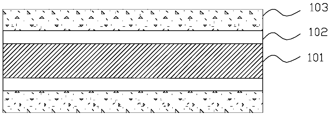
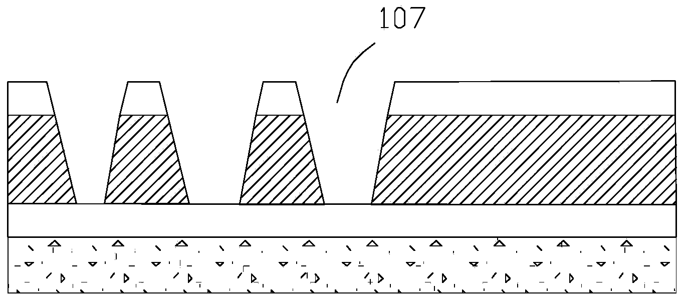
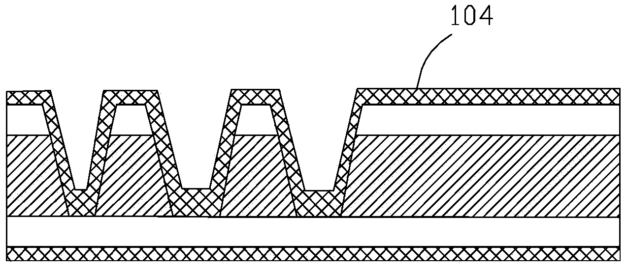
[0042] refer to Figure 1-7 , a method for preparing a high-density packaging substrate hole-mounted product, comprising the following steps:

[0043] Cutting—baking plate—making positioning holes—removing the upper surface protective layer—laser drilling—microetching—removing the lower surface protective layer—removing glue—depositing chemical copper—MSAP process—— Electroplating and hole filling - MSAP film removal - MSAP etching - post process.

[0044] Among them, the substrate materials used for cutting are such as figure 1 As shown (the thin copper substrate includes a dielectric layer 101, a copper foil 102 and a protective film layer 103). Different from the traditional copper-clad substrate material, the thickness of the substrate is 0.1mm, and the outer side of the copper foil (thickness is 2-4μm) has a layer of protective copper foi...


PUM

PropertyMeasurementUnit
Thicknessaaaaaaaaaa
Thicknessaaaaaaaaaa
Copper thicknessaaaaaaaaaa

Abstract

The invention discloses a high-density package substrate on-hole disk product and a preparation method of the high-density package substrate on-hole disk product. The preparation method comprises the following steps of drying a substrate, manufacturing locating holes, conducting laser drilling, conducting micro-etching, conducting copper plating, conducting pattern transfer, conducting electroplating for hole filling and conducting film stripping and etching, and then the high-density package substrate on-hole disk product is obtained. According to the method, under the effect of protective film layers of the thin copper substrate, the problem that copper foil at the bottom is cut through in the thin copper processing process in the past is solved, and a complete half-through hole structure is made on the thin copper substrate; meanwhile, the direct laser processing technology is adopted, the thickness of the copper foil can not be influenced, and through good matching between the direct laser processing technology and the MSAP process, a high-density Flip-chip product with the high-flatness on-hole disk structure can be manufactured.

Description

technical field [0001] The invention relates to the technical field of printed circuit board production, in particular to a plate-on-hole product of a high-density packaging substrate and a preparation method thereof. Background technique [0002] As a carrier of semiconductor chips, one of the main functions of the packaging substrate is the transition structure between the chip and the circuit board. In order to meet the requirements of higher density packaging, packaging products with ultra-thin Flip-chip structure have aroused widespread interest in the industry and have developed rapidly in recent years. Compared with the traditional Wire-bonding structure, the feature of the Flip-chip structure packaging substrate is that the connection points are changed from the peripheral distribution to the planar array distribution, and the connection method with the chip is also changed from the traditional gold / copper wire to the small size solder ball. This technology of array...

Claims


Application Information

Patent Timeline
IPC IPC(8): H05K1/11H05K3/42H05K3/00
CPCH05K1/11H05K3/00H05K3/42H05K1/113H05K3/425H05K2201/10674
Inventor 王名浩谢添华李志东
Owner GUANGZHOU FASTPRINT CIRCUIT TECH
Why Eureka
Try Eureka