

Method for improving electrical resistivity evenness of P-type silicon epitaxial wafer for CCD
A technology of silicon epitaxial wafers and resistivity, which is applied in semiconductor/solid-state device manufacturing, circuits, electrical components, etc., can solve the difficulties of P-type epitaxial layers and affect the uniformity of resistivity of epitaxial layers, etc., so as to promote the development process and improve Effect of Resistivity Uniformity
- Summary
- Abstract
- Description
- Claims
- Application Information
AI Technical Summary
Problems solved by technology
Method used
Image

Examples
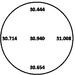
Embodiment 1
[0023] Example 1: (1) First use the base silicon coating technology, the method is: use HCl gas to etch the base of the epitaxial furnace to remove the residual deposits on the base, the etching temperature is set to 1150 ° C, the purity of the HCl gas ≥99.99%, the flow rate is set to 1L / min, the etching time is set to 3min, and then the base is covered with a layer of intrinsic polysilicon, the growth material is trichlorosilane gas, the purity is ≥99.95%, and the flow rate is set to 35 g / min, the growth time was set to 10min.
[0024] (2) Put a P-type silicon substrate in the pit of the base. The silicon wafer has a crystal orientation of , a resistivity of 0.01 Ω·cm, a thickness of 450 μm, and a diameter of 100 mm. The selected silicon substrate has a shallow back damage layer on the back, and the back damage layer is coated with polysilicon and silicon dioxide to form a back seal layer, and the damage density of the back damage shallow layer is controlled at 6×10 6 piece / ...
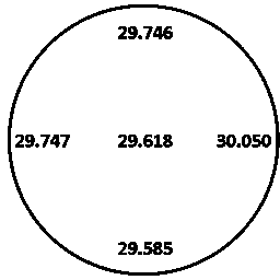
Embodiment 2
[0033] Example 2: (1) First use the silicon-coated base technology. The method is: use HCl to etch the base of the epitaxial furnace to remove the residual deposits on the base. The etching temperature is set at 1170°C, and the purity of HCl gas is ≥ 99.99%, the flow rate is set to 1L / min, the etching time is set to 5 min, and then the base is covered with a layer of intrinsic polysilicon, the growth material is trichlorosilane gas, the purity is ≥99.95%, and the flow rate is set to 30 g / min, the growth time was set to 10min.
[0034] (2) Put a P-type silicon substrate in the pit of the pedestal. The silicon wafer has a crystal orientation of , a resistivity of 0.01 Ω·cm, a thickness of 450 μm, and a diameter of 100 mm. The selected silicon substrate has a shallow back damage layer on the back, and the back damage layer is coated with polysilicon and silicon dioxide to form a back seal layer, and the damage density of the back damage shallow layer is controlled at 6×10 6 piec...
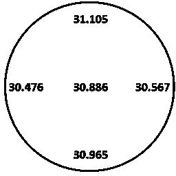
Embodiment 3
[0043] Example 3: (1) First use the base silicon coating technology, the method is: use HCl gas to etch the base of the epitaxial furnace to remove the residual deposits on the base, the etching temperature is set to 1170 ° C, the purity of the HCl gas ≥99.99%, the flow rate is set to 1L / min, the etching time is set to 3min, and then the base is covered with a layer of intrinsic polysilicon, the growth material is trichlorosilane gas, the purity is ≥99.95%, and the flow rate is set to 35 g / min, the growth time was set to 10min.
[0044] (2) Put a P-type silicon substrate in the pit of the base. The silicon wafer has a crystal orientation of , a resistivity of 0.01 Ω·cm, a thickness of 450 μm, and a diameter of 100 mm. The selected silicon substrate has a shallow back damage layer on the back, and the back damage layer is coated with polysilicon and silicon dioxide to form a back seal layer, and the damage density of the back damage shallow layer is controlled at 6×10 6 piece / ...
PUM
| Property | Measurement | Unit |
|---|---|---|
| thickness | aaaaa | aaaaa |
| diameter | aaaaa | aaaaa |
Abstract
Description
Claims
Application Information