

Preparation method of spherical superfine gold powder for electronic materials
An electronic material and spherical technology, which is applied in the field of preparation of spherical ultrafine gold powder for electronic materials, can solve the problems of morphology and structure characteristics, unsatisfactory tap density and particle size, etc.
- Summary
- Abstract
- Description
- Claims
- Application Information
AI Technical Summary
Problems solved by technology
Method used
Image

Examples
Embodiment
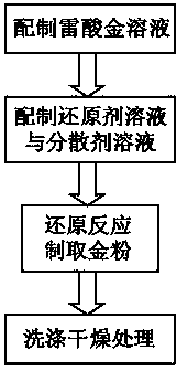
[0019] The specific preparation method is as follows:
[0020] a) Prepare gold fulminate solution. The specific preparation process is: first put a certain amount of gold nuggets in a dissolving container, add a small amount of deionized water, heat slightly, then add appropriate amount of aqua regia several times to dissolve the gold nuggets, and wait for the gold nuggets to dissolve. After it is completely dissolved, add concentrated hydrochloric acid several times to catch the nitrate; when there is no brown smoke, add deionized water several times to catch the acid; when there is no pungent smell, concentrate the solution to a concentration of 30 g / L for later use. Then add ammonia water to the gold solution to adjust the pH value to weak alkaline, so as to fully form the gold fulminate solution; finally adjust the pH value of the gold fulminate solution to 3.5 with hydrochloric acid.
[0021] b) Prepare reducing agent solution and dispersant solution. The specific prepara...
PUM
 Abstract
Description
Claims
Application Information