Crystal lattice dislocation detecting method

A dislocation and lattice technology, applied in the field of integrated circuit design, can solve problems such as electrical failure and find the location of dislocations, and achieve the effect of improving efficiency

Active Publication Date: 2015-01-21
SHANGHAI HUAHONG GRACE SEMICON MFG CORP
View PDF7 Cites 3 Cited by
  • Summary
  • Abstract
  • Description
  • Claims
  • Application Information

AI Technical Summary

Problems solved by technology

Dislocations can also cause electrical failures. Due to the need for failure analysis of the cause of device failure, it is often difficult to know in advance whether it is caused by dislocations, and it is difficult to find the location of dislocations through physical analysis.

Method used


Image

  • Crystal lattice dislocation detecting method
  • Crystal lattice dislocation detecting method
  • Crystal lattice dislocation detecting method

Examples


Embodiment Construction

[0020] The method for detecting lattice dislocations described in the present invention comprises the following steps:

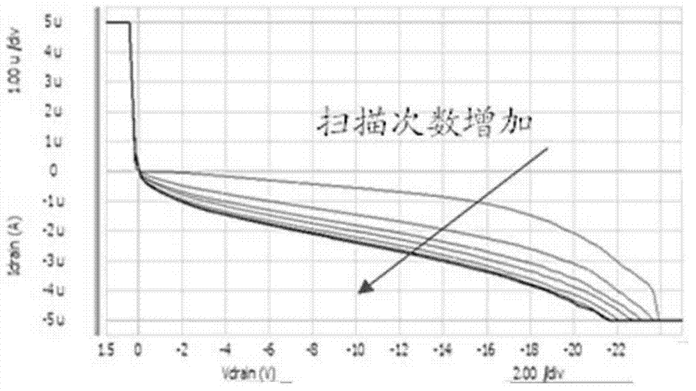
[0021] The first step is to select failed devices for electrical testing, such as MOS tubes, diodes, triodes, memory tubes, etc. The voltage-current curve was measured by multiple scans. If it is a storage tube that cannot measure the voltage-current curve, read the current of the storage tube multiple times to detect changes in the current. Observe whether the voltage-current curve (storage tube is the current curve, the same below) obtained by multiple scans gradually becomes larger or smaller, such as figure 2 The voltage-current curve shown is for a pLDMOS I dss Taking failure analysis as an example, the curves obtained by scanning multiple measurements are different and have changed.

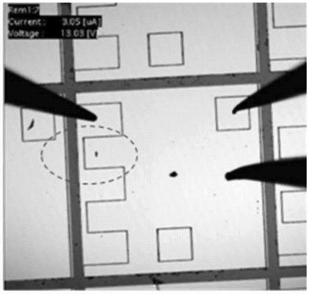
[0022] The second step is to bake the failed device and re-measure its voltage-current curve several times to observe whether it gradually becomes larger or smaller. ...


PUM

PropertyMeasurementUnit
Lengthaaaaaaaaaa
Thicknessaaaaaaaaaa

Abstract

The invention discloses a crystal lattice dislocation detecting method. The method comprises the steps that an invalid device is selected for carrying out an electrical test, a voltage-current curve of the invalid device is scanned and measured repeatedly, and whether the voltage-current curve obtained through repeated scanning becomes larger or smaller is observed; the invalid device is roasted, the voltage-current curve of the invalid device is repeatedly measured again, and whether the voltage-current curve becomes larger or smaller is observed; if it is determined that the voltage-current curve of the device is changed, emission microscope positioning is carried out, and the dislocation range is reduced further; the device is ground, a focused ion beam is used for cutting the device, and a transmission electron microscope sample is formed through physical analytical sample preparation; a common transmission electron microscope observation way is adopted for dislocation observation to obtain a dislocation image. According to the crystal lattice dislocation detecting method, the dislocation is analyzed and the dislocation position is found from the electrical analysis process to the physical analysis process, the integrated circuit device invalidation analysis efficiency is improved, and the cost is reduced.

Description

technical field [0001] The invention relates to the field of integrated circuit design, in particular to a method for detecting lattice dislocations in integrated circuit failure analysis. Background technique [0002] During the manufacturing process of integrated circuit chips, dislocations appear inside the chip due to stresses that occur during temperature unevenness, lattice mismatch, doping, deposition, etc. The so-called dislocation refers to an internal microscopic defect of a crystalline material, that is, a local irregular arrangement of atoms (crystallographic defect). From a geometric point of view, dislocation is a kind of line defect, which can be regarded as the dividing line between the slipped part and the non-slip part in the crystal. Its existence has a great influence on the physical properties of materials, especially the mechanical properties. Such as figure 1 As shown, it is a typical location where dislocations are likely to occur, such as dislocati...

Claims


Application Information

Patent Timeline
IPC IPC(8): G01R31/28G01Q30/20G01Q30/02
Inventor 马香柏
Owner SHANGHAI HUAHONG GRACE SEMICON MFG CORP
Why Eureka
Try Eureka