High-level copper circuit board and manufacturing method thereof

A circuit board production and circuit board technology, which is applied in the direction of printed circuit manufacturing, printed circuit, printed circuit parts, etc., can solve the problems of thin solder resist ink for thick copper lines, difficulty in improving the yield rate, and air bubbles in the dry film, and achieve Improve the yield rate, improve thermal management performance, and avoid the effects of film bubbles

Active Publication Date: 2017-06-30
KALEX MULTI LAYER CIRCUIT BOARD (ZHONGSHAN) CO LTD
View PDF13 Cites 0 Cited by
  • Summary
  • Abstract
  • Description
  • Claims
  • Application Information

AI Technical Summary

Problems solved by technology

Because of the unevenness of the surface, it brings challenges to the production of surface circuits. At the same time, it is more difficult to improve the yield rate, and the line beach position is relatively large at the critical point where the high and low copper is scattered and handed over. Disadvantages of Thin Solder Resist Ink for Thick Copper Lines

Method used


Image

  • High-level copper circuit board and manufacturing method thereof
  • High-level copper circuit board and manufacturing method thereof
  • High-level copper circuit board and manufacturing method thereof

Examples


Embodiment 1

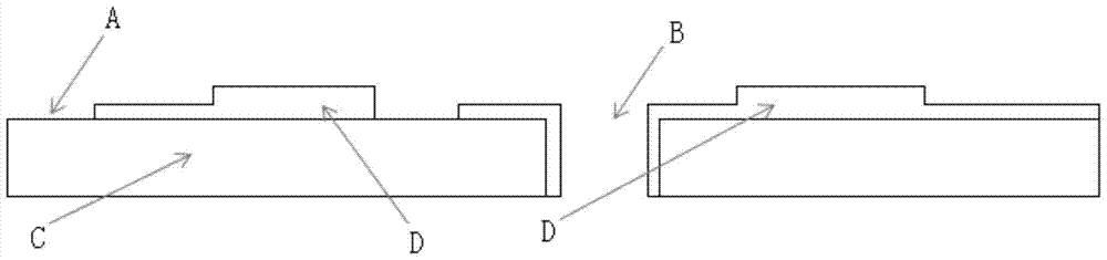
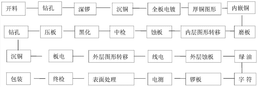
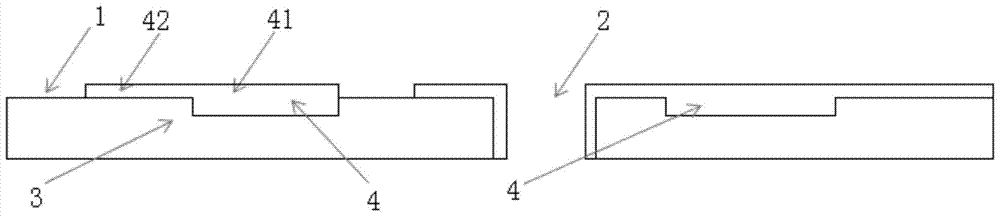
[0046] A kind of 2OZ / 12OZ high step copper circuit board (multi-panel) manufacturing method, according to figure 2 The process flow shown proceeds as follows:

[0047] (1) Pre-process: Including cutting, drilling and other processes, it is produced according to the conventional process.

[0048] (2) Deep gong: Before work, measure the flatness of the operation table to control the operation table at a horizontal height, and detect the warpage of the circuit board that requires deep gong to ensure that the warpage does not exceed 0.4%. Then place the inner layer of the multi-layer board horizontally, use a gong machine to deep-drill the inner layer according to the preset thick copper line direction and depth, and drill thick copper line slots on the circuit board that are consistent with the preset thick copper line direction.

[0049] The gong machine is placed on a platform made of cement and cushioning materials after the ground has been compacted, and the weight of the g...

Embodiment 2

[0067] A kind of 1OZ / 3OZ high step copper circuit board (double panel) manufacturing method, according to Figure 4 The process flow shown proceeds as follows:

[0068] (1) Pre-process: Including cutting, drilling and other processes, it is produced according to the conventional process.

[0069] (2) Deep gong: Before work, measure the flatness of the operation table to control the operation table at a horizontal height, and detect the warpage of the circuit board that requires deep gong to ensure that the warpage does not exceed 0.4%. Then place the inner layer of the multi-layer board horizontally, use a gong machine to deep-drill the inner layer according to the preset thick copper line direction and depth, and drill thick copper line slots on the circuit board that are consistent with the preset thick copper line direction.

[0070] The gong machine is placed on a platform made of cement and cushioning materials after the ground has been compacted, and the weight of the g...

Embodiment 3

[0092] The manufacturing method of the high-step copper circuit board of the present embodiment is basically the same as the manufacturing method of Embodiment 1, the difference is that:

[0093] The circuit board is a 1OZ / 12OZ high-level copper circuit board.

[0094] (3) Copper sinking: the process parameters of the degumming process are: KMnO 4 The concentration is 50g / L, and the degumming rate is 0.4g / cm 2 .

[0095] The copper sinking process parameters are: 33°C, Cu2 + The concentration is 2.4g / L, the concentration of HCHO is 4.5g / L, the concentration of NaOH is 13g / L, and the copper precipitation rate is 0.10g / cm 2 .

[0096] (6) Embedded copper: use the following copper paste screen printing process to embed copper in the thick copper line groove: fill the conductive copper paste into the thick copper line groove by screen printing, the specific process is: the screen printing angle is 5 -15 degrees, the pressure of the scraper is 20-30Kg / cm 2 , The screen printi...


PUM


Abstract

The invention discloses a high-step copper circuit board and a manufacturing method thereof, belonging to the technical field of circuit board manufacturing. The method includes deep gongs, copper sinking, full board electroplating, embedded copper, grinding board, pattern transfer and etching processes. In this method, a thick copper line slot is firstly drilled at the position of the thick copper line on the circuit board, and then the thick copper line slot is embedded in the copper layer, and then the surface stepped copper line is made through the grinding plate and pattern transfer process, that is, through the deep The gongs and thick copper and thin copper are plated at the same time to achieve perfect wiring, and the uneven surface of the stepped copper is embedded in the circuit board. The circuit board produced by this method, because the high-current copper plating is directly embedded in the resin, there is no problem of uneven surface, on the one hand, the availability of the layout space of the circuit board is improved, and on the other hand, it is also avoided. Problems such as film bubbles caused by graphics transfer, thereby improving the yield rate of the product.

Description

technical field [0001] The invention relates to the technical field of circuit board production, in particular to a high-level copper circuit board and a production method thereof. Background technique [0002] With the improvement of people's living standards, the requirements for the environment are getting higher and higher, the awareness of energy conservation and the sense of energy crisis are getting stronger and stronger, and the voice of accelerating the research and development of hybrid electric vehicles is getting louder and louder. At the same time, the cost performance and marketization degree of hybrid electric vehicles are more and more widely concerned by people. Furthermore, in order to meet the multi-functional technical requirements of hybrid electric vehicle circuit boards, electronic technology is also constantly developing and innovating electronic components for high-end hybrid electric vehicles, and accelerating the pace of hybrid electric vehicles to...

Claims


Application Information

Patent Timeline
Patent Type & Authority Patents(China)
IPC IPC(8): H05K1/09H05K3/00
Inventor 戴匡
Owner KALEX MULTI LAYER CIRCUIT BOARD (ZHONGSHAN) CO LTD
Why Eureka
Try Eureka