Preparation method of metal bonding pad in through hole of SOI sheet

A manufacturing method and technology for metal pads, applied in the field of micro-processing, can solve the problems of difficult pad manufacturing, high processing cost, and difficulty in retaining photoresist, so as to be suitable for mass production, less equipment requirements, and simple equipment. Effect

Active Publication Date: 2015-02-04
INST OF ELECTRONICS CHINESE ACAD OF SCI
View PDF5 Cites 3 Cited by
  • Summary
  • Abstract
  • Description
  • Claims
  • Application Information

AI Technical Summary

Problems solved by technology

[0013] The spin-coated photoresist process is a commonly used method, but considering that the SOI base layer has been opened, the spin-coated photoresist is difficult to survive on the highly patterned surface, and the photoresist is too thick at the bottom of the pit. It cannot be removed by exposure, so patterned transfer cannot be realized, and the required pads cannot be made
The three-dimensional glue spraying process can not be limited by the highly patterned surface, but this process requires special dry film deposition equipment, and the processing cost is relatively high
Moreover, photolithography on the patterned surface belongs to proximity exposure, and the problem of light diffraction caused by it also affects the accuracy of photolithography to a certai

Method used


Image

  • Preparation method of metal bonding pad in through hole of SOI sheet
  • Preparation method of metal bonding pad in through hole of SOI sheet
  • Preparation method of metal bonding pad in through hole of SOI sheet

Examples


Embodiment Construction

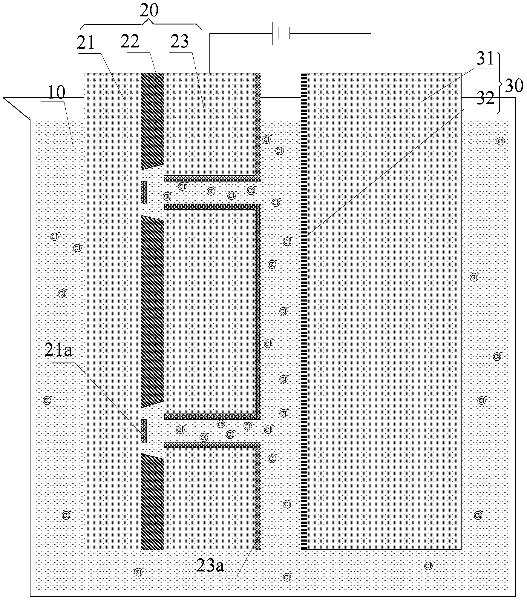
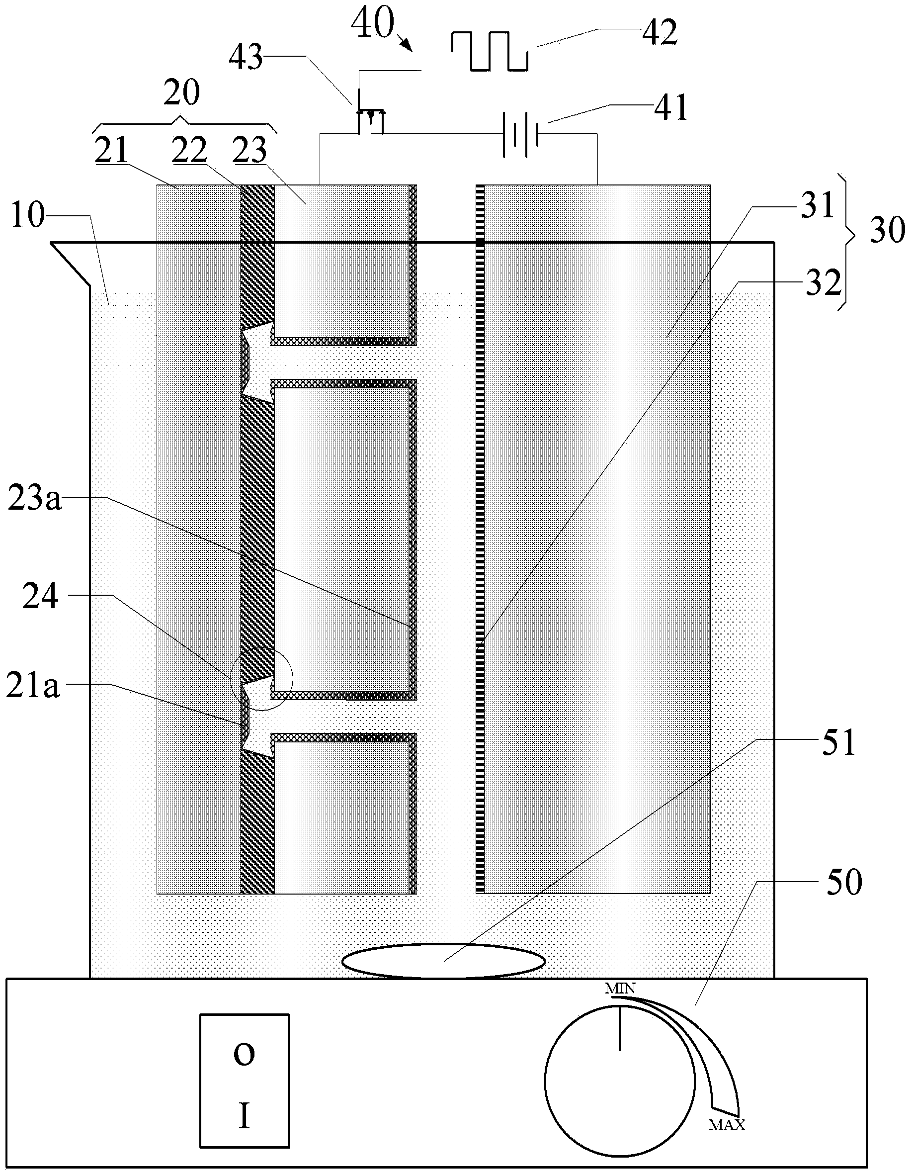
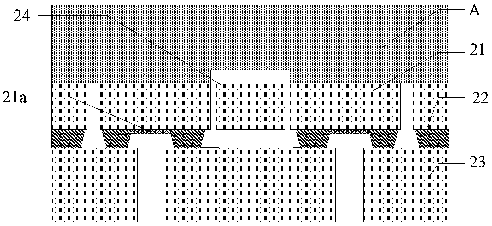
[0044] In order to make the object, technical solution and advantages of the present invention clearer, the present invention will be further described in detail below in conjunction with specific embodiments and with reference to the accompanying drawings. It should be noted that, in the drawings or descriptions in the specification, similar or identical parts all use the same figure numbers. Implementations not shown or described in the accompanying drawings are forms known to those of ordinary skill in the art. Additionally, while illustrations of parameters including particular values ​​may be provided herein, it should be understood that the parameters need not be exactly equal to the corresponding values, but rather may approximate the corresponding values ​​within acceptable error margins or design constraints.

[0045] The invention utilizes the special three-layer structure of the SOI sheet and adopts an electrochemical corrosion method to realize the fabrication of t...


PUM


Abstract

The invention provides a preparation method of a bonding pad in a through hole in MEMS (Micro-electromechanical System) wafer-level vacuum package. According to the preparation method, a special structure of the through hole in an SOI substrate is utilized, and the bonding pad in the through hole is prepared by adopting an electrochemical corrosion method, so that the problem of electrical short circuit of back metal in a base layer of the SOI sheet is effectively solved, and the preparation method has the advantages of being low in cost, suitable for volume production and the like.

Description

technical field [0001] The invention relates to the technical field of micromachining, in particular to a method for manufacturing a metal pad in a through hole of an SOI chip in a MEMS wafer-level vacuum package. Background technique [0002] Micro-Electro-Mechanical System (MEMS) is a high-tech cutting-edge discipline developed on the basis of integrating various micro-processing technologies and applying the latest achievements of modern information technology. It has a wide range of applications in almost all fields that people come into contact with. prospect. [0003] Vacuum packaging plays a vital role in MEMS micro-sensors. On the one hand, it can protect the movable parts in the micro-sensor, making it not easy to damage; on the other hand, it can isolate the external environment (such as gas, humidity, dust, etc.), making Gyroscopes, accelerometers, pressure sensors, RF switches, etc. will work fine. Vacuum packaging can be divided into shell-level and wafer-leve...

Claims


Application Information

Patent Timeline
IPC IPC(8): B81C1/00
Inventor 王军波谢波陈德勇
Owner INST OF ELECTRONICS CHINESE ACAD OF SCI
Why Eureka
Try Eureka