Terahertz/laser lamination detector
A detector, terahertz technology, applied to detectors in multispectral composite detection, multimode field, to achieve the effect of small size, good conductivity, and simplified overall structure
- Summary
- Abstract
- Description
- Claims
- Application Information
AI Technical Summary
Problems solved by technology
Method used
Image
Examples
Embodiment 1
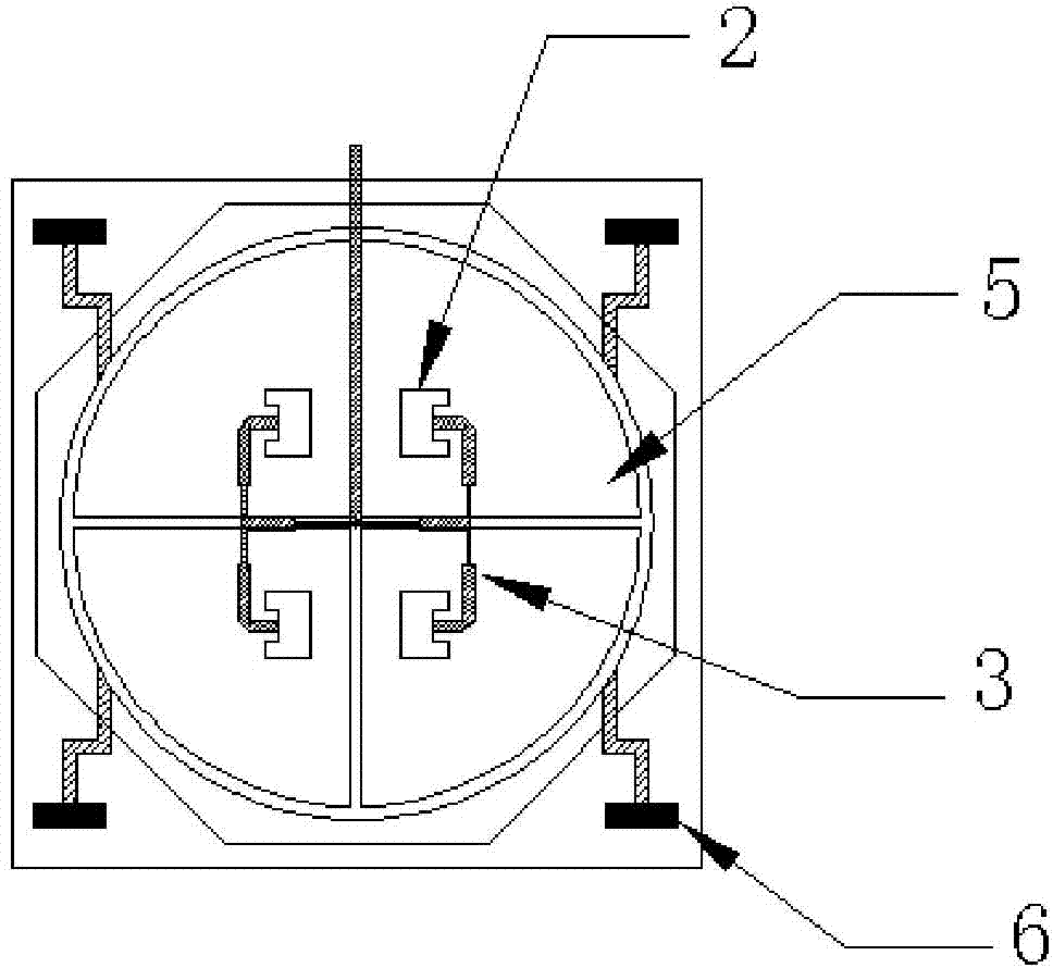
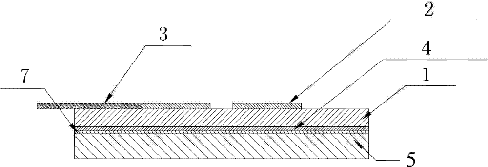
[0023] figure 1 , figure 2 Shown is a terahertz / laser stacked detector shown in Example 1. The dual-mode stacked detector is composed of a microstrip antenna and a four-quadrant laser detector, wherein the microstrip antenna is formed by an insulating dielectric substrate 1 The upper conductive film patch 2, the metal feeder 3, and the conductive film ground plate 4 under the insulating dielectric substrate 1 are formed. The conductive film ground plate 4 of the microstrip antenna is pasted on the four sides by an infrared-transmitting adhesive 7. On the surface of the quadrant laser detector 5 , the four-quadrant laser detector outputs signals through metal electrodes. The conductive film patch is a 2*2 array, symmetrically distributed according to the center of the detector. The conductive film patches in each array are connected to a metal feed line. The conductive film is a graphene film, and the graphene film is made of three layers of graphene film. The metal feeder...
Embodiment 2
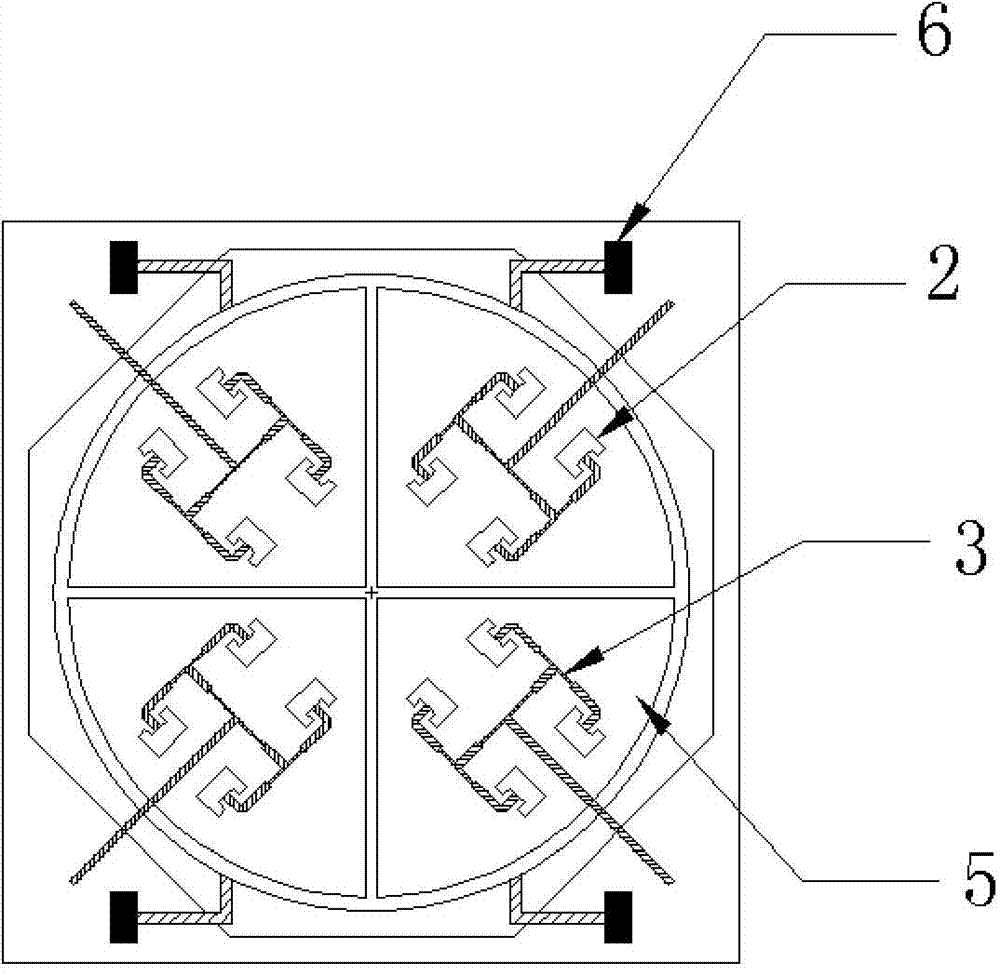
[0026] image 3 It is a terahertz / laser laminated detector shown in Embodiment 2. The conductive thin film patch is a 4*4 array, which is composed of four conductive thin film patches in a 2*2 array.
[0027] The patch size and arrangement of the microstrip antenna are related to the required THz frequency and the number of elements of the antenna, and are set according to specific conditions.
[0028] The concrete preparation process of embodiment 2 is as follows:
[0029] 1. The insulating dielectric substrate 1 is sapphire with a thickness of 0.2 mm, the graphene film patch 2 is a 4×4 patch array pattern, and the material of the metal feeder 3 is chromium / gold. According to the shape of the designed patch antenna, a photolithographic pattern is prepared, including a photolithographic plate for preparing a feeder pattern and a photolithographic pattern for preparing an antenna pattern.
[0030] 2. A single-layer graphene film is grown on a copper foil substrate with chemic...
PUM
| Property | Measurement | Unit |
|---|---|---|
| Thickness | aaaaa | aaaaa |
Abstract
Description
Claims
Application Information


