

Organic semiconductor material, preparation method and electroluminescent device
A technology of electroluminescent devices and organic semiconductors, applied in the fields of organic semiconductor materials, preparation, and electroluminescent devices, can solve problems such as shortages, achieve high thermal stability, improve luminous efficiency, and the effect of simple and easy synthesis methods
- Summary
- Abstract
- Description
- Claims
- Application Information
AI Technical Summary
Problems solved by technology
Method used
Image

Examples
preparation example Construction
[0026] The invention provides a kind of preparation method of organic semiconductor material, comprises the steps:
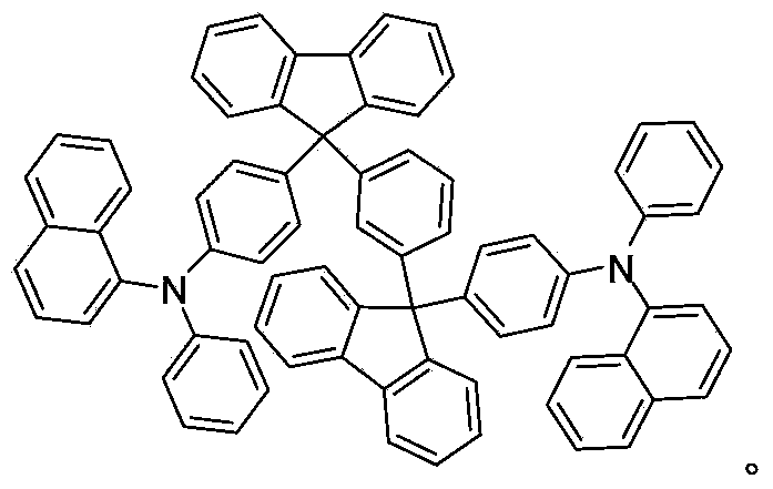
[0027] Provides compound A: and compound B: Under an inert atmosphere, first dissolve compound A in an organic solvent, then add compound B, an inorganic base and a catalyst to the organic solvent containing compound A and react at 70-120°C for 6-15 hours, the compound A The molar ratio to compound B is 1:2 to 1:2.4, and the chemical formula of the organic semiconductor material obtained by stopping the reaction is as follows:
[0028]
[0029] The preparation method of the organic semiconductor material further includes a post-processing step. The post-processing step specifically includes: using n-hexane as eluent to separate and purify the organic semiconductor material obtained by stopping the reaction through a silica gel layer, and vacuum drying to obtain the target product.
[0030] The condition of the vacuum drying is drying at 50-70° C. for 12-2...
Embodiment 1
[0041] N,N'-(4,4'-(9,9'-(1,3-phenylene)bis(9H-fluorene-9,9-diyl))bis(4,1-phenylene))bis (N-phenylnaphthyl-1-amine) preparation process preparation steps are as follows:
[0042]
[0043] Under nitrogen protection, 1,3-bis(9-(4-tetrabromophenyl)-9H-fluoren-9-yl)benzene (57.3g, 80mmol) was dissolved in 200mL N,N-dimethylformamide (DMF) solution, then added N-phenylnaphthalene-1-amine (35.0g, 160mmol), potassium carbonate (22.1g, 160mmol) and cuprous iodide (1.52g, 8mmol). The reactants were stirred and reacted at 120° C. for 6 hours. Stop the reaction and cool to room temperature, filter, and wash the solid three times with distilled water to obtain the product N,N'-(4,4'-(9,9'-(1,3-phenylene)bis(9H-fluorene-9,9 -diyl))bis(4,1-phenylene))bis(N-phenylnaphthyl-1-amine), and then use the eluent n-hexane to separate by silica gel column chromatography, and then dry at 50°C under vacuum for 24h An off-white solid was obtained. The yield was 83%.
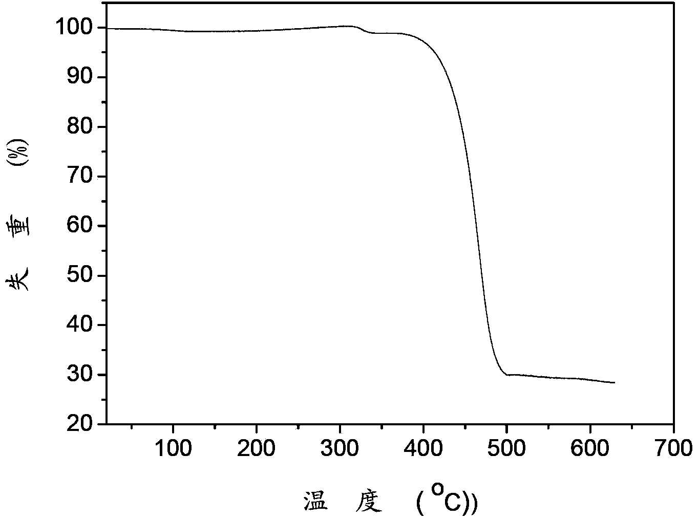
[0044] Experimental test dat...
Embodiment 2
[0048] N,N'-(4,4'-(9,9'-(1,3-phenylene)bis(9H-fluorene-9,9-diyl))bis(4,1-phenylene))bis (N-phenylnaphthyl-1-amine) preparation process preparation steps are as follows:
[0049]
[0050] Under nitrogen protection, 1,3-bis(9-(4-tetrabromophenyl)-9H-fluoren-9-yl)benzene (57.3g, 80mmol) was dissolved in 200mL toluene (Tol) solution, and then added N-Phenylnaphthalen-1-amine (38.5g, 176mmol), cesium carbonate (57.2g, 176mmol), copper powder (0.768g, 12mmol). The reactants were stirred and reacted at 110° C. for 9 hours. Stop the reaction and cool to room temperature, filter, and wash the solid three times with distilled water to obtain the product N,N'-(4,4'-(9,9'-(1,3-phenylene)bis(9H-fluorene-9,9 -diyl))bis(4,1-phenylene))bis(N-phenylnaphthyl-1-amine), and then use the eluent n-hexane to separate by silica gel column chromatography, and then dry at 50°C under vacuum for 24h An off-white solid was obtained. The yield was 81%.
PUM
 Abstract
Description
Claims
Application Information