
Method for preparing narrow frame display device

A display device, narrow frame technology, applied in optics, instruments, nonlinear optics, etc., can solve problems such as poor reliability, poor sealing strength, liquid crystal puncture, etc., to achieve good display performance and stability, and enhanced bonding strength. Effect

Active Publication Date: 2018-01-19
BEIJING BOE OPTOELECTRONCIS TECH CO LTD
View PDF7 Cites 0 Cited by
  • Summary
  • Abstract
  • Description
  • Claims
  • Application Information

AI Technical Summary

Problems solved by technology

However, the sealing strength obtained by this method is poor, and problems such as puncture of liquid crystal, precipitation of pollutants, and poor reliability are prone to occur.

Method used


Image

  • Method for preparing narrow frame display device
  • Method for preparing narrow frame display device
  • Method for preparing narrow frame display device

Examples


Embodiment

[0047] Taking PI solution (polyimide AL-00010) as an example to carry out radiation modification.

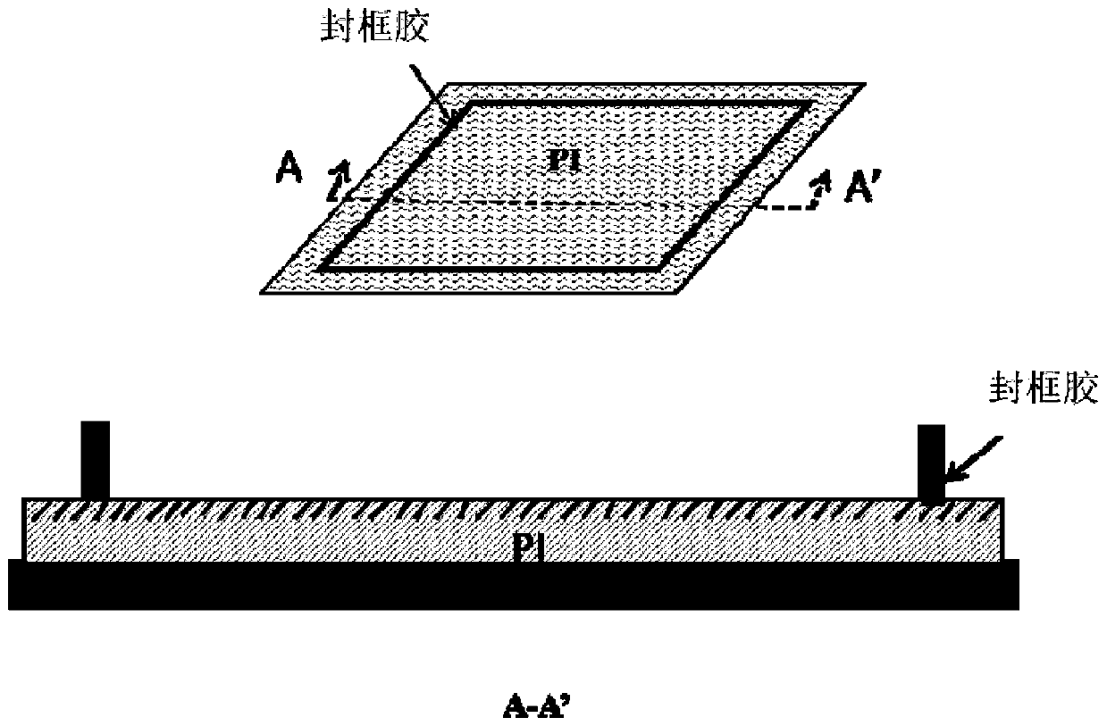
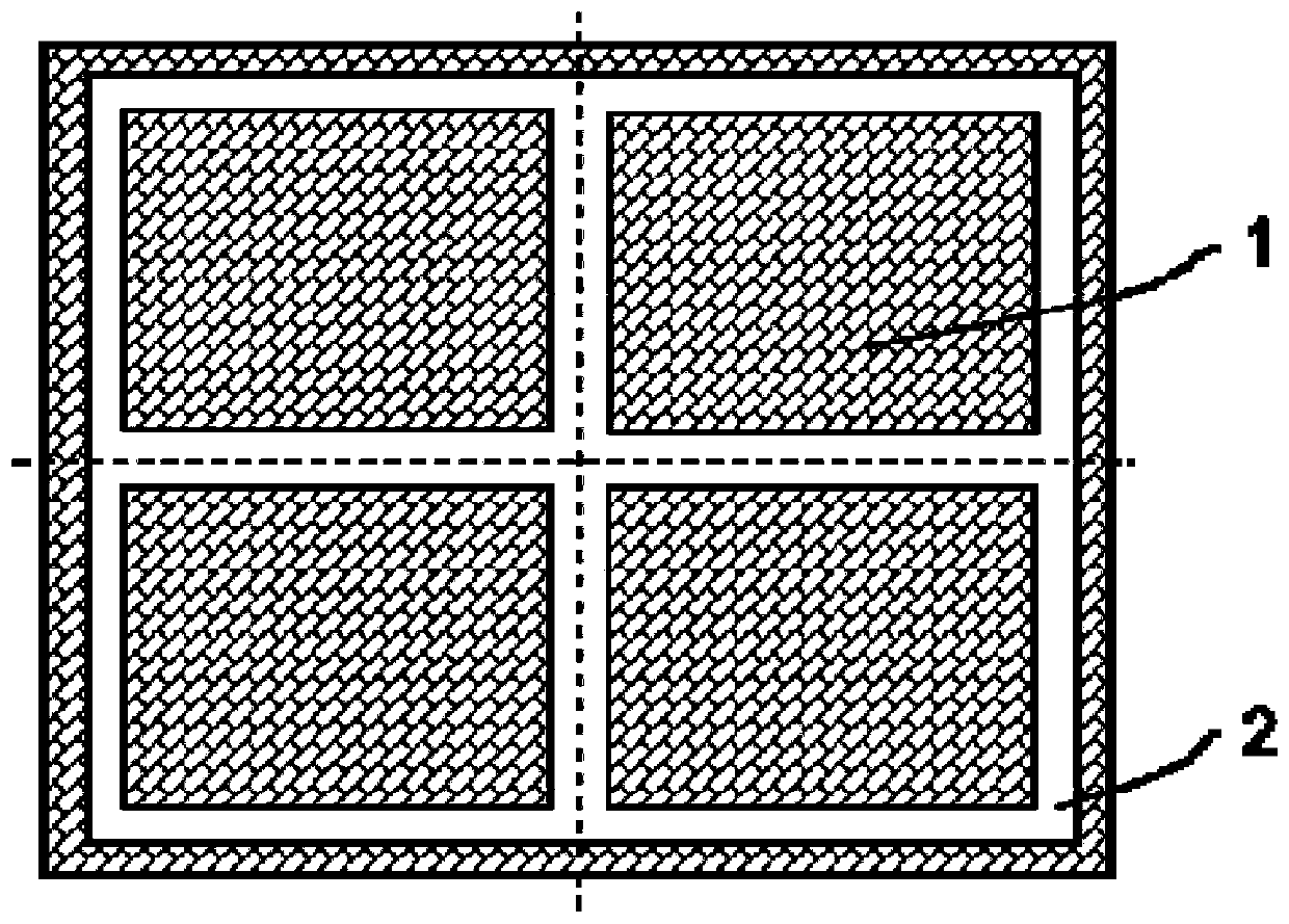
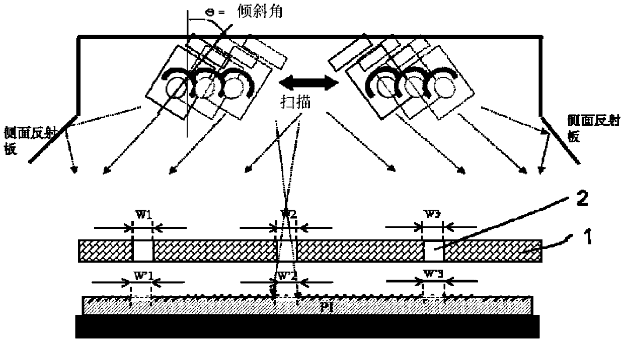
[0048] Using conventional methods in the field, the above PI liquid is coated on the array substrate to form a PI film, which is subjected to rubbing alignment treatment. The array substrate that has undergone orientation treatment is placed on the stage in the radiation precursor. Rotate the stage and adjust the position of the radiation shield so that the part of the array substrate to be treated with radiation (sealing position) is aligned with the light-transmitting part of the radiation shield.

[0049] Among them, the radiation source is an ultraviolet lamp, the wavelength of the linear ultraviolet light emitted is 254nm, and the radiation intensity is 1.0J / cm 2 .

[0050] The radiation modification process of the above PI film is shown in the following schematic diagram:

[0051]

[0052] a. The cleavage reaction of the ester group on the branched chain of the PI fi...


PUM

PropertyMeasurementUnit
wavelengthaaaaaaaaaa
strengthaaaaaaaaaa
wavelengthaaaaaaaaaa

Abstract

A method for manufacturing a display apparatus comprises: performing radiation processing on a polyimide film at a sealed position of a substrate, so as to make the polyimide film at the sealed position of the substrate generate a free radical; and coating frame sealing glue at the sealed position, and performing consolidation. By performing radiation processing on a polyimide film, a cracking reaction of a surface group of the polyimide film occurs to generate a free radical; mutual reactions can occur between the free radical and an active group of the frame sealing glue, so that the bonding strength is increased, and the problems such as liquid crystal puncture, liquid crystal pollution and poor reliability are avoided.

Description

technical field [0001] The invention relates to the field of display technology, in particular to a method for preparing a narrow frame display device. Background technique [0002] Due to its small size, low power consumption, and no radiation, liquid crystal displays (LCDs) have become the mainstream products in flat panel displays, and the requirements for slimness and light weight are increasing day by day. [0003] The narrow frame design of the display device is a trend in the development of the display field. At present, the narrow frame design methods of TFT-LCD (Thin Film Transistor LCD) display products are mostly realized by overlapping polyimide film (PI film) and sealing glue (Seal). However, due to the poor adhesion between the PI film and the frame sealant, it is easy to have poor reliability, such as weak adhesion, and afterimage problems caused by pollution precipitates caused by poor compatibility. Uncontrollable factors make it difficult for narrow borde...

Claims


Application Information

Patent Timeline
Patent Type & Authority Patents(China)
IPC IPC(8): G02F1/1339G02F1/1337G02F1/1333
CPCG02F1/1333G02F1/1339G02F1/13398G02F1/1303G02F2202/023
Inventor 李建张伟李鸿鹏宋省勳
Owner BEIJING BOE OPTOELECTRONCIS TECH CO LTD
Learn More